
Accelerate your semiconductor packaging failure analysis
Transform your workflows with best-in-class imaging, efficient sample preparation and characterization with ZEISS microscopy solutionsIn the More-than-Moore era, the semiconductor industry demands smaller, faster, and more powerful devices, driving the critical role of semiconductor packaging.
The complex packaging architectures, feature scaling and increasing density of interconnects have introduced challenges in reliability, fault isolation and physical analysis.
ZEISS offers new workflows and improves the throughput, success rate and yield with innovative breakthroughs in non-destructive imaging, high throughput sample preparation and best-in-class imaging and analysis capabilities.

ZEISS workflow solutions overview
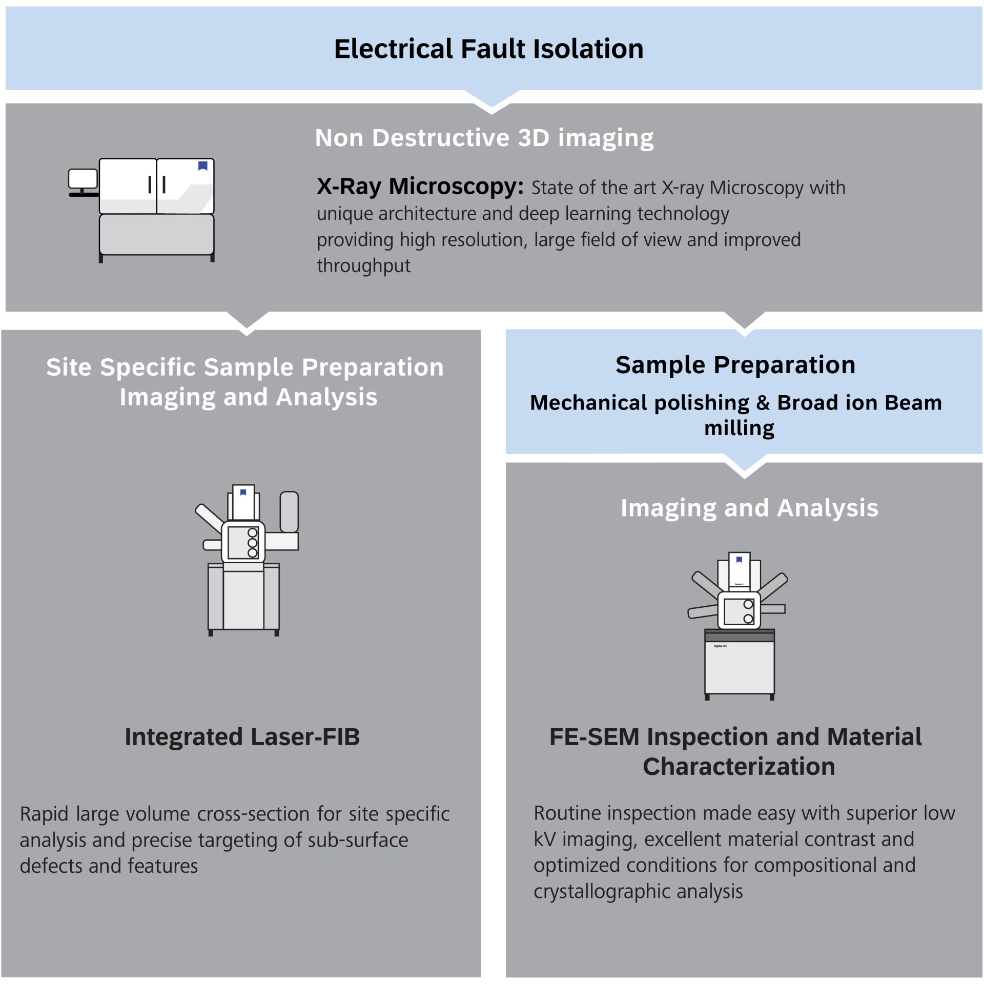
Here's how we can helpFault isolation and physical analysis workflows have seen new challenges with the advances in semiconductor packaging technology.
Innovative connected workflows and correlative solutions from ZEISS address some of these new challenges and increase throughput and success rate.
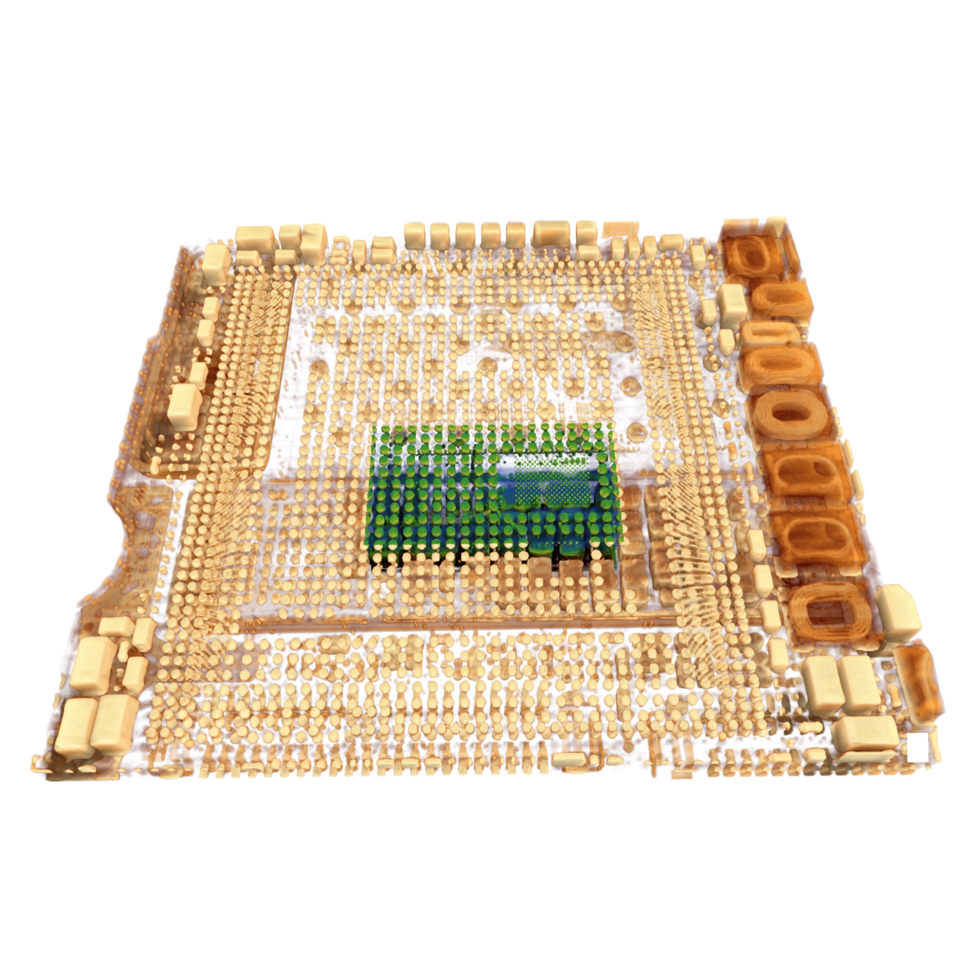
Non-destructive 3D Imaging
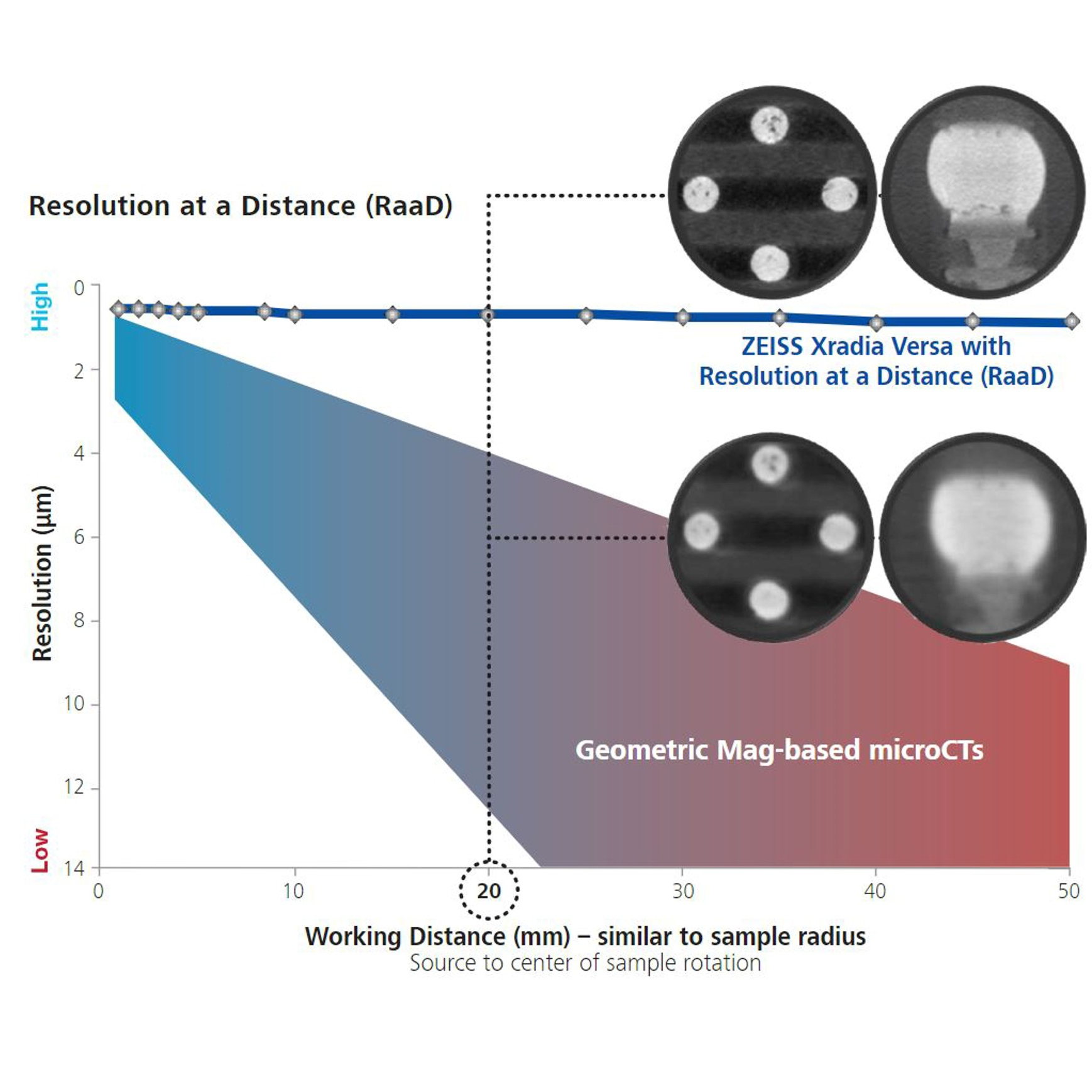
ZEISS X-ray microscopy enables non-destructive high-resolution visualization of several defects and failure modes, minimizing physical analysis for known defects. Physical cross-sectioning, imaging and materials analysis is often required for new defects and failure modes. Depending on the failure mode and analysis requirements, conventional sample preparation methods or site-specific rapid sample preparation may be required for root cause analysis.
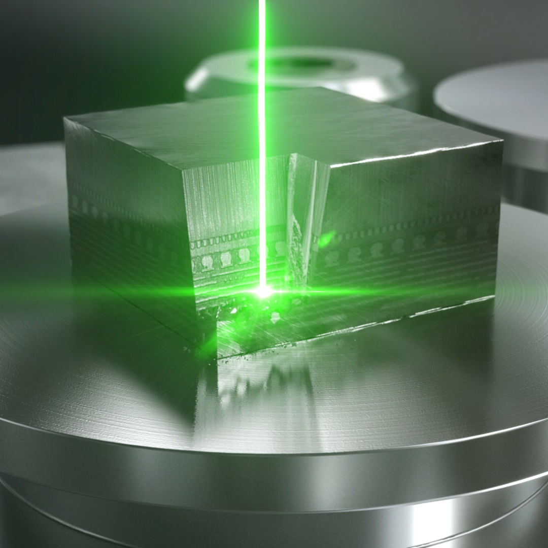
Site Specific Failure Analysis
Site-specific sample preparation guided by the X-ray data using the laser-integrated FIB-SEM enables fast and precise sample preparation. This workflow is tailored to enhance productivity and turnaround time within minutes compared to hours.
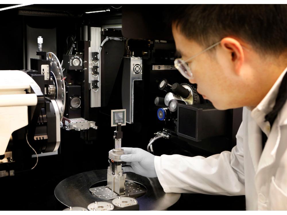
Routine Imaging and Analysis
Sample preparation using conventional mechanical polishing and broad ion beam milling is still relevant for several cases. The optical and X-ray imaging data can be used to direct sample preparation and fed to the ZEN software for fast and easy navigation in ZEISS electron microscopes for routine inspection and analysis
Learn more by interacting with the flashing blue dots below.
Transform your sample prep and site-specific analysis with efficient workflows

Learn more about this workflow below
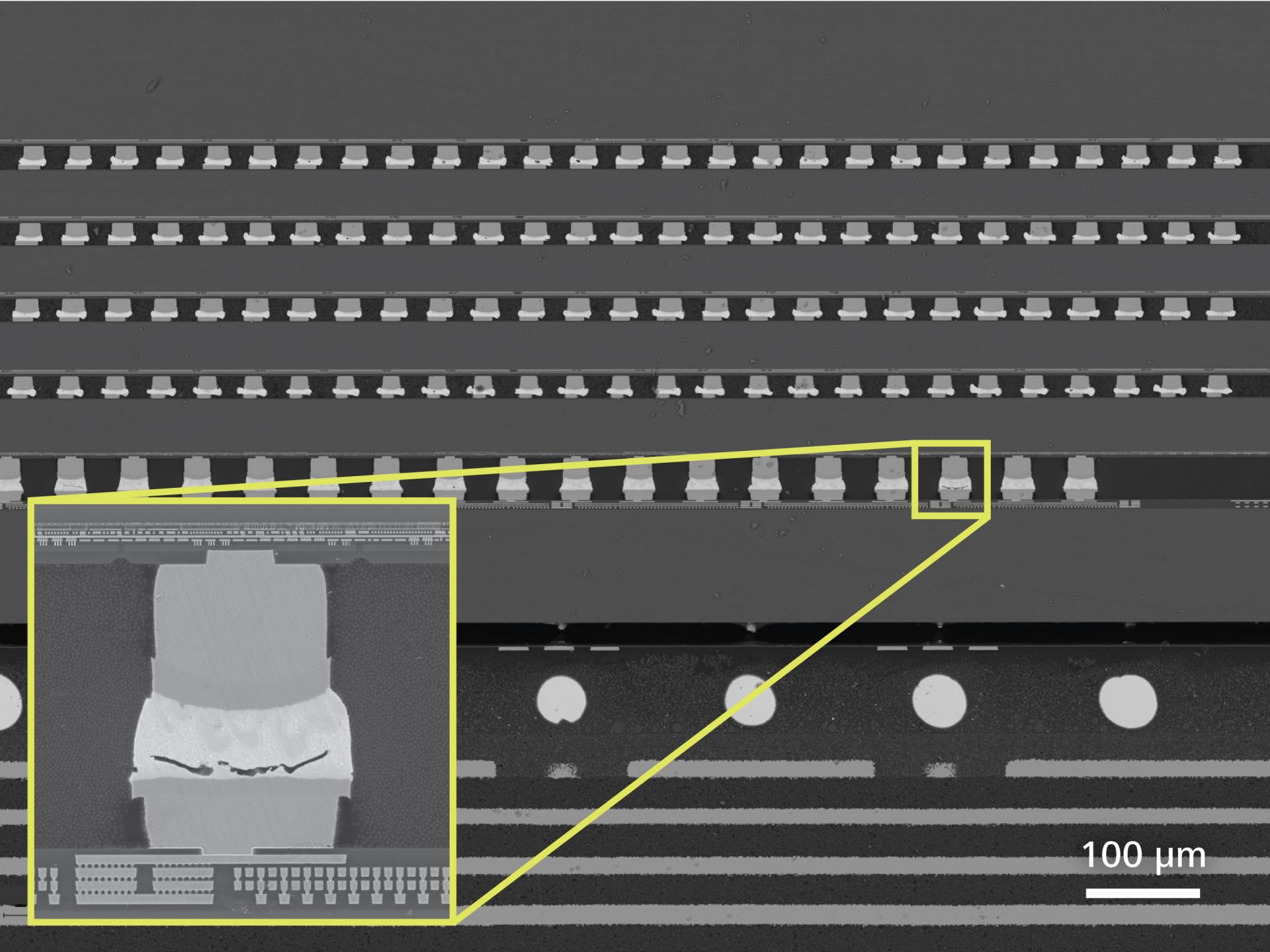
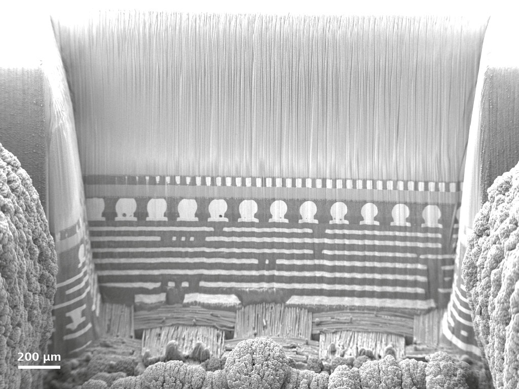
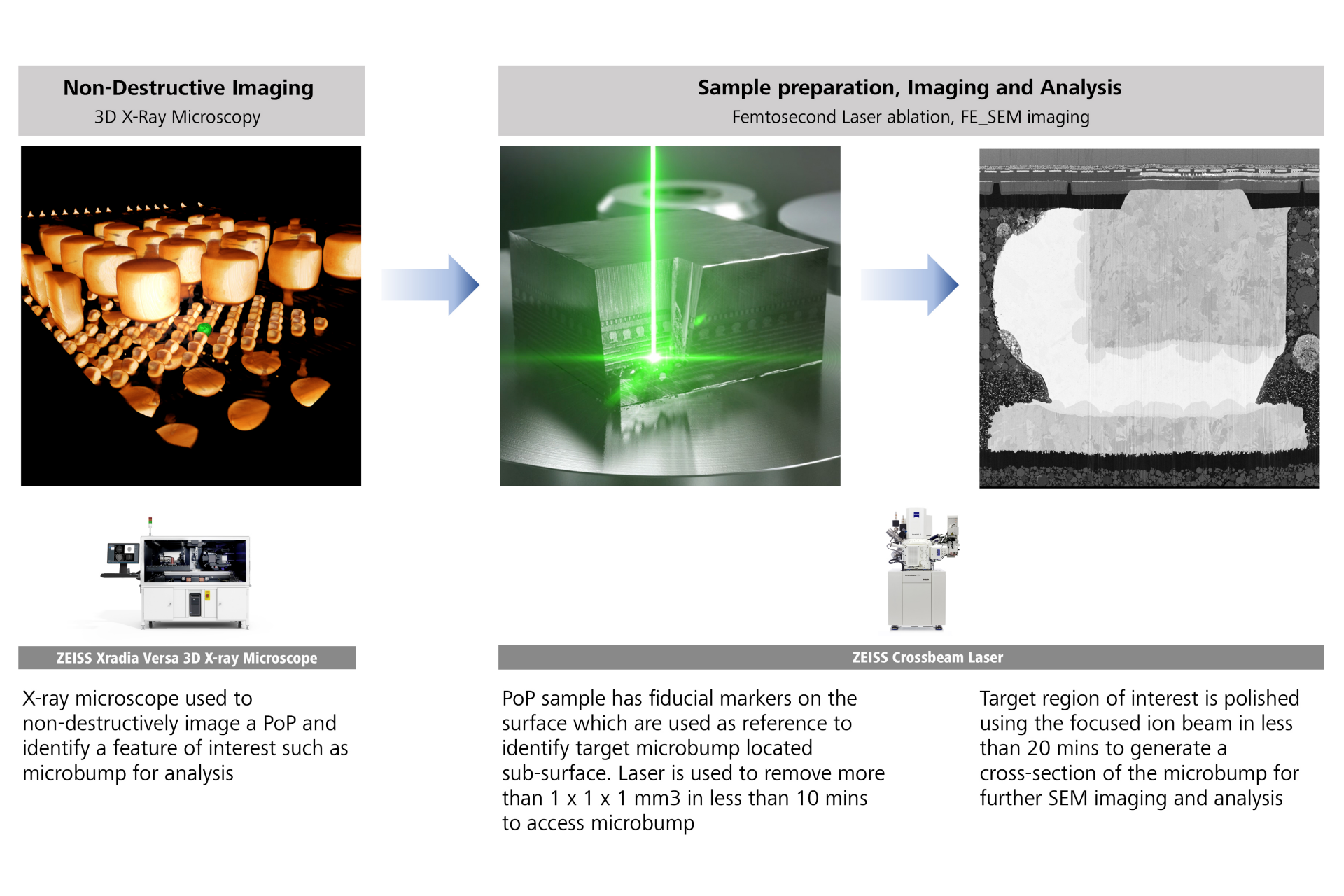
Advanced package failure analysis using correlated X-ray microscopy and LaserFIB
The evolution of packaging architecture with increasing density and scaling of features is resulting in large footprints to accommodate more components and functions that are integral in the heterogeneous integration roadmap and the More-than-Moore era.
These developments pose new challenges in failure analysis and process characterization and drive need for advances in analysis tools, techniques, and development of novel workflows. In this work, we discuss the advances in two classes of techniques that have gained traction in the advanced packaging industry, 3D X-Ray Microscopy (XRM) and laser-integrated focused ion beam scanning electron microscopes (FIB-SEM) for sample preparation.
While the laser integration in the FIB-SEM workflows has improved cross-section preparation throughput, precise targeting for site specific analysis of buried features requires the correlation with a complementary technique to provide sub-surface information.
The use of 3D XRM to guide laser-integrated FIB-SEM analysis presents several advantages to address this challenge. In this work, we describe a novel workflow using 3D XRM and fs-laser integrated in a FIB-SEM (also called a LaserFIB) to precisely target and deliver results at high throughput. This represents a significant development in addressing the challenges of advanced package failure analysis.
Learn more by interacting with the flashing blue dots below.
3D X-ray guided sample preparation for routine inspection
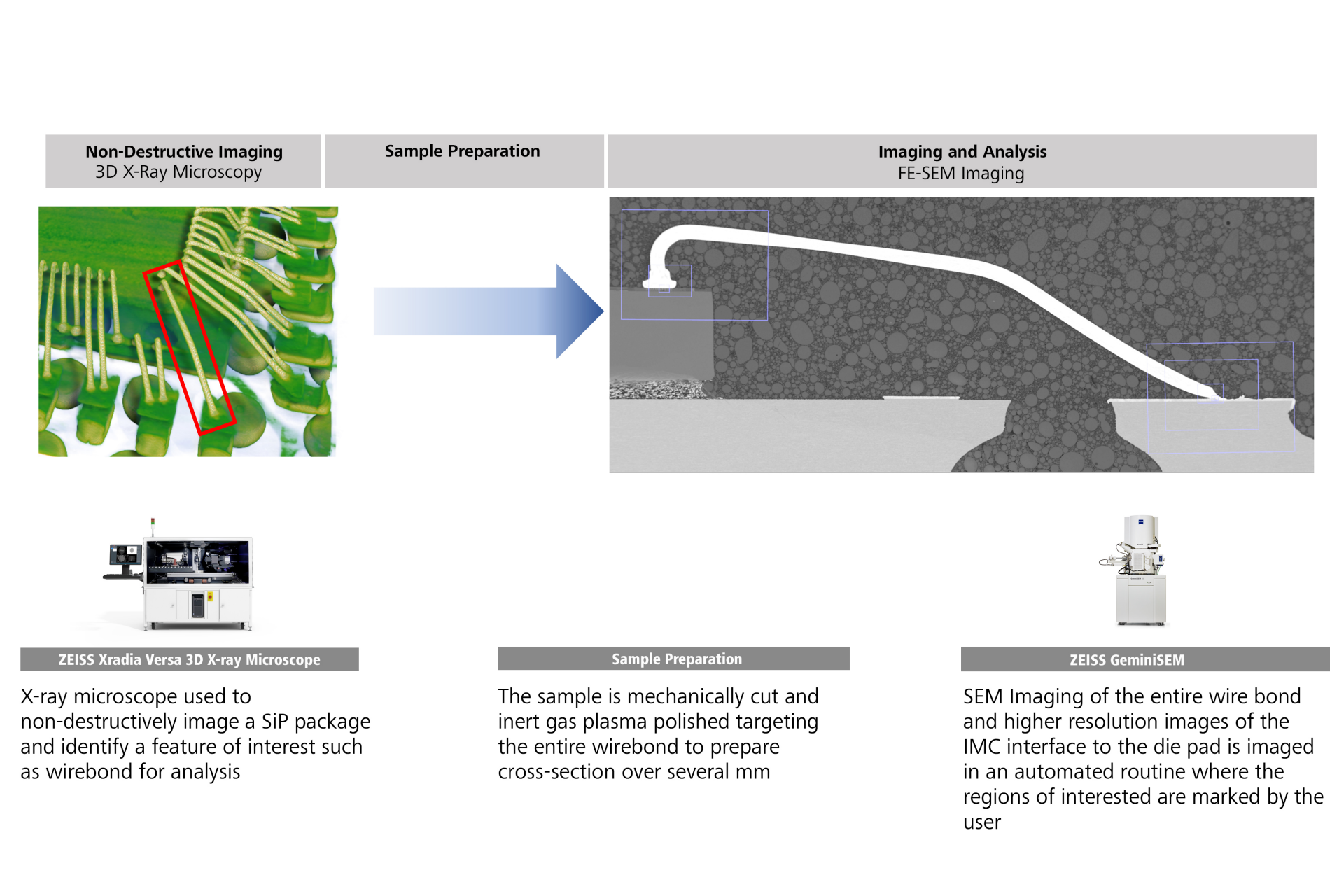

Learn more about this workflow below
Do you identify with any of these problems?

Are you limited by the resolution of your non-destructive techniques to isolate and visualize defects in your large package?

Are you challenged by the poor contrast of your X-ray CT to see underfill voids, delamination and cracks?