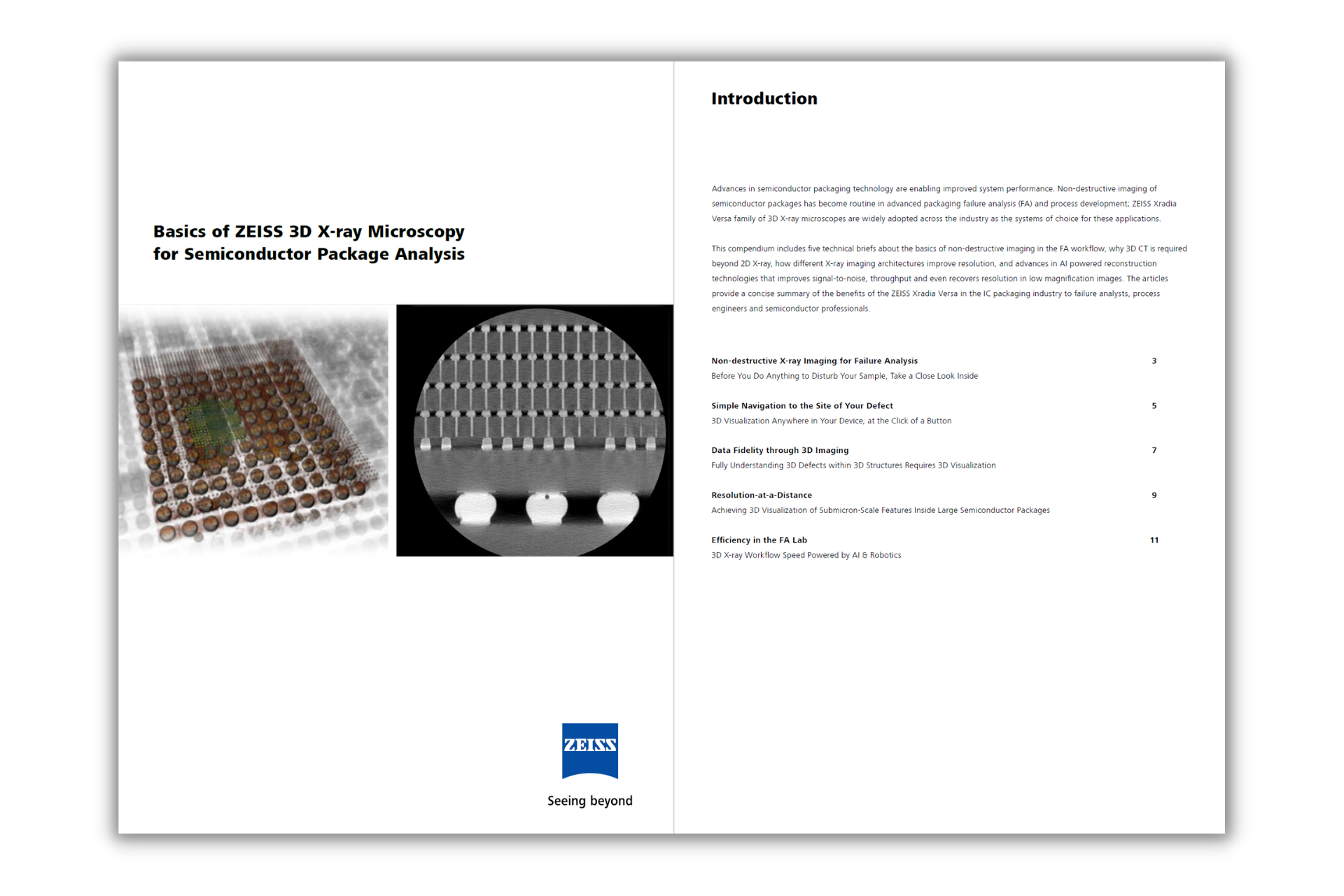

Learn how to use ZEISS XRM to improve success rates & efficiency for semiconductor package failure analysis
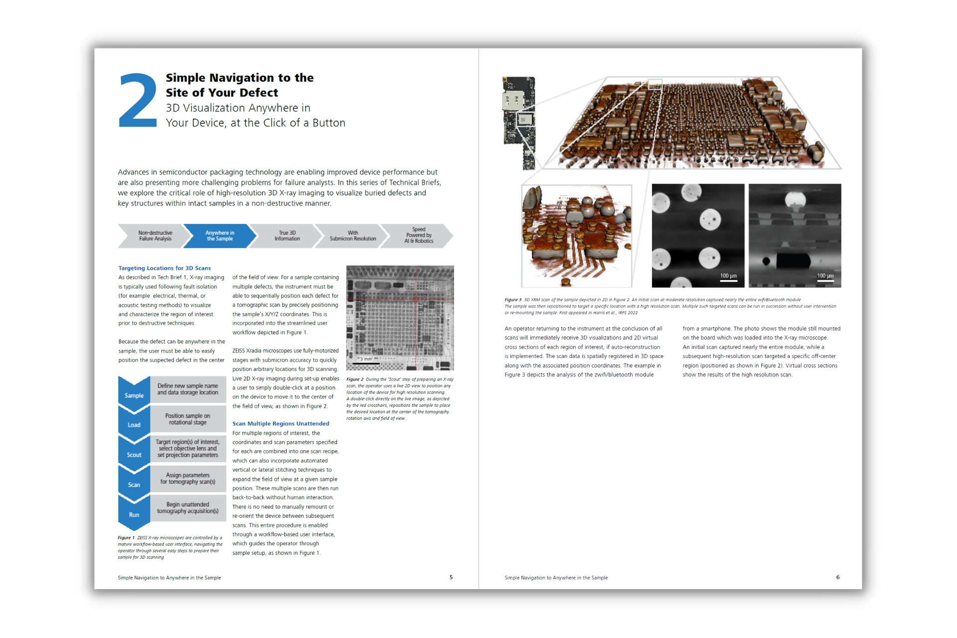
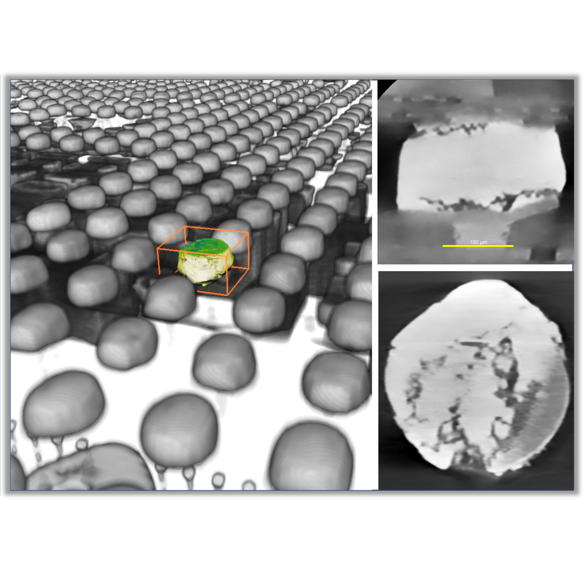
Visualize in 3D without altering your defectWhile searching for the root cause of problems in your device,
3D X-ray microscopy can help you…

Achieve breakthrough resolution with cutting edge XRM technology
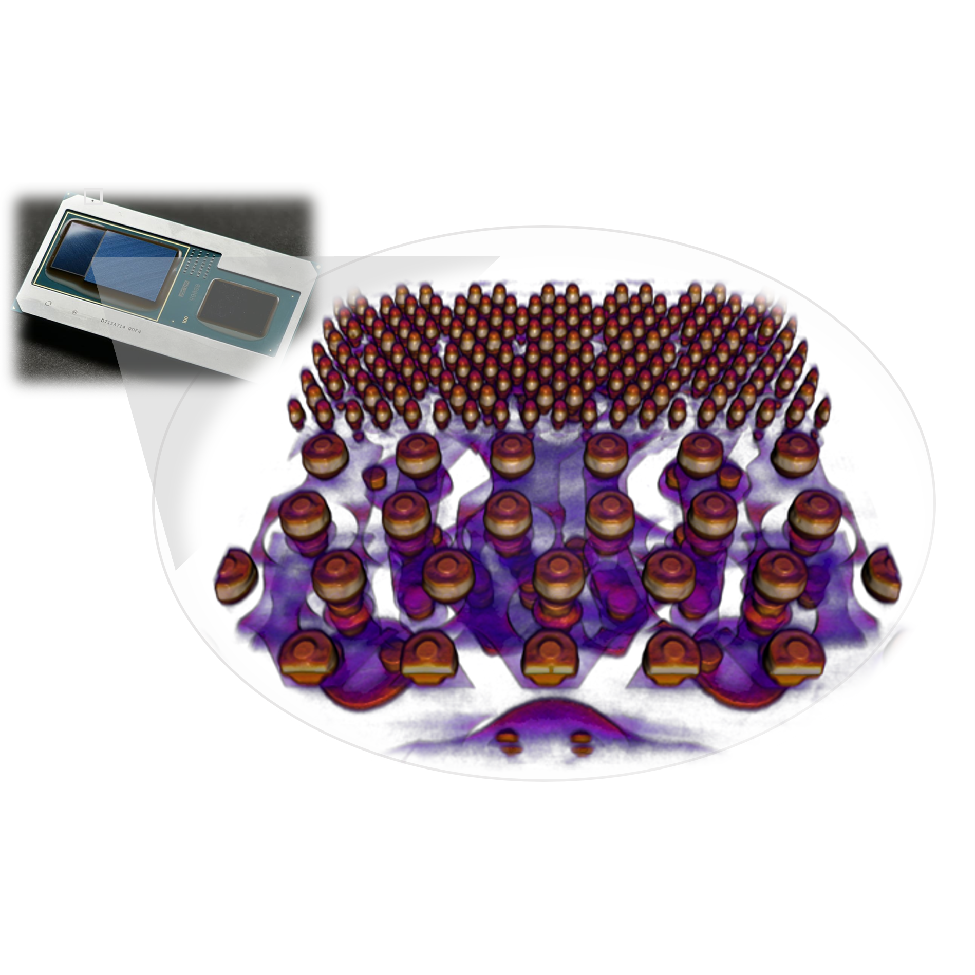
The semiconductor packaging industry is moving towards smaller and high density of interconnects with heterogeneous integration resulting in large package size.
Non-destructive imaging of these large packages with high-resolution pushes the limits of current X-ray microscopy and CT equipment.
The next-generation Xradia 630 Versa extends the frontiers of submicron-resolution 3D imaging and analysis, enabling unprecedented 450 nm spatial resolution up to 160kV X-ray energy.

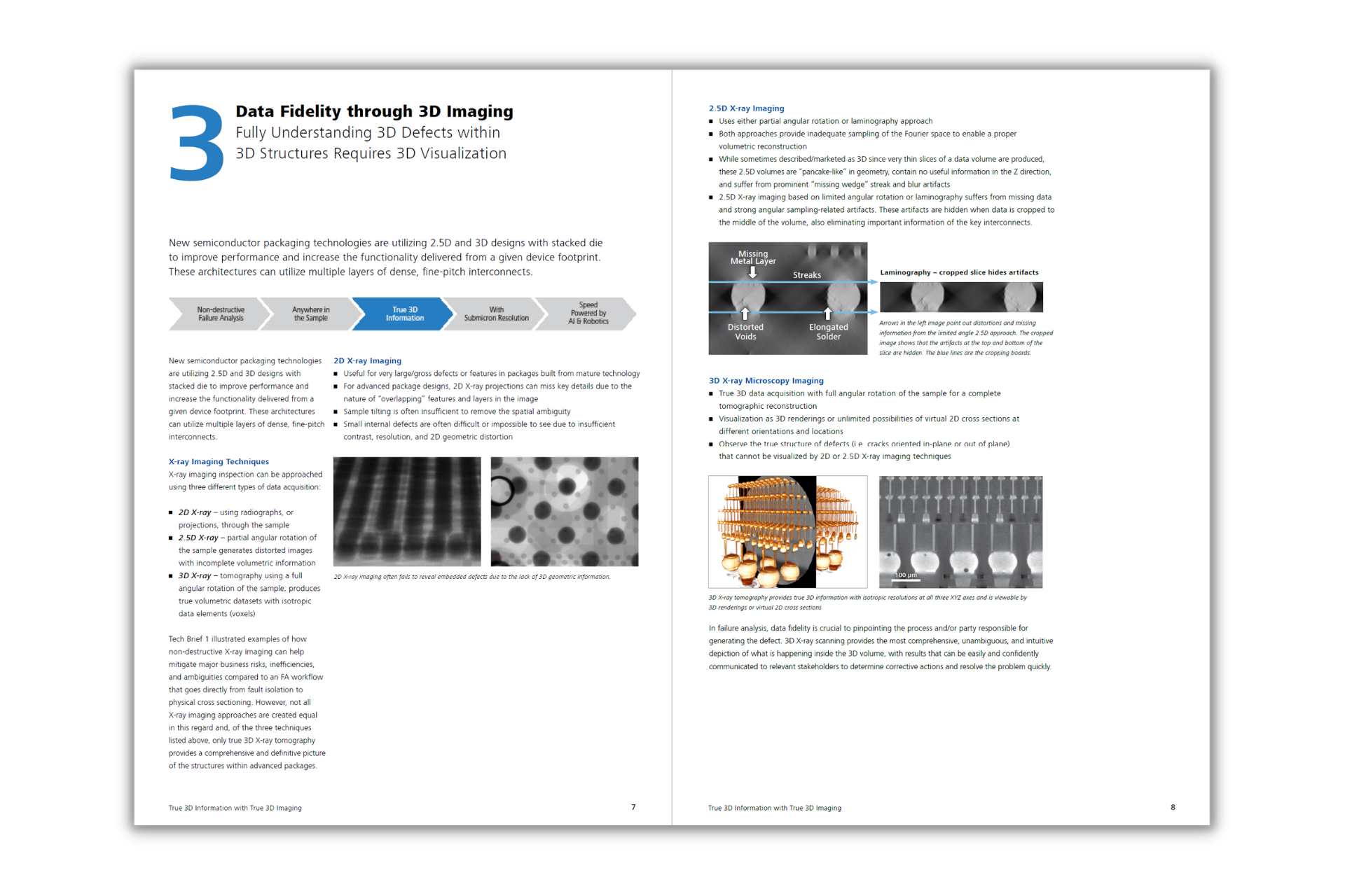
Architecture that provides superior contrast even for diverse materials
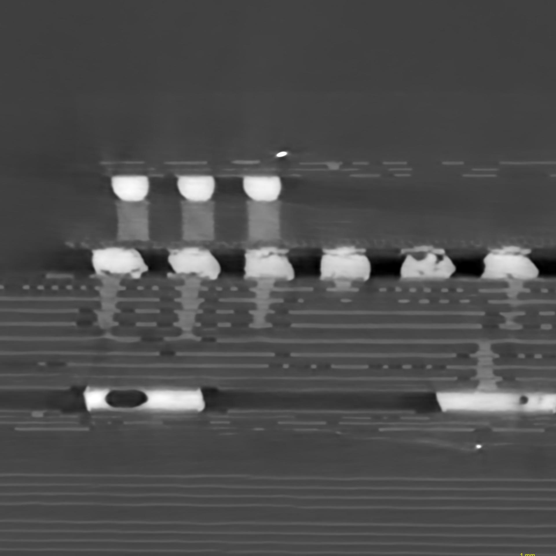
Diverse materials used in semiconductor packaging, such as polymers, resins, adhesives, thermal interface materials, and several other soft materials in addition to metal wires, traces, solder where visualization can be difficult due to their low contrast.
ZEISS Xradia Versa microscopes are designed with a unique architecture employing advanced scintillator coupled optics that provide superior contrast even for soft materials. This combined with resolution at a distance capability provides high resolution with high contrast in comparison to conventional X-ray CT.


AI-based reconstruction for high-throughput
Without compromising on image qualitySome of the fundamental challenges in X-ray imaging such as high resolution at fast acquisition time and high-resolution at large field view are now being addressed with innovative AI based technologies.
Advanced reconstruction using deep learning, ZEISS DeepRecon Pro and DeepScout can provide more than 4X improvement in throughput, image quality and resolution recovery over large field of view.
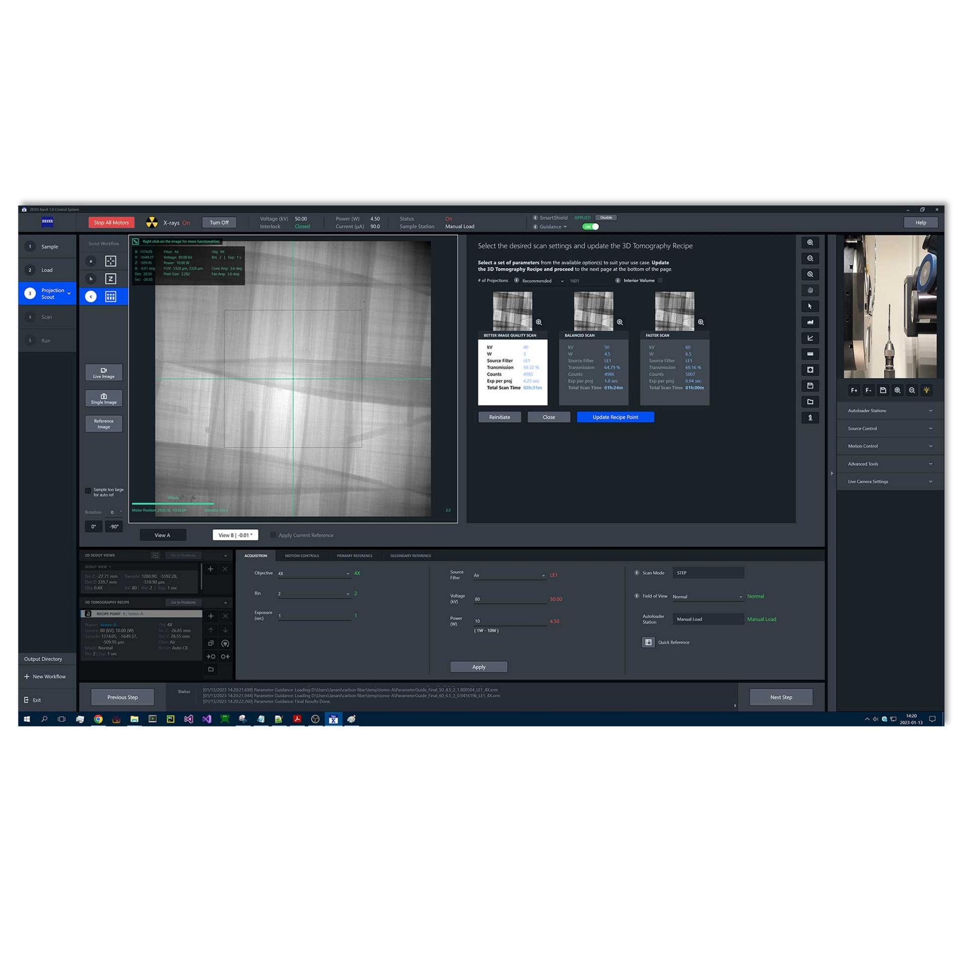

Effortless navigation: An integrated user-centric interface
NavX user interfaceZEISS NavX™, the new user interface for ZEISS Xradia 630 Versa, guides users through automated workflows with intelligent system insights and delivers experimental results more easily and efficiently while also allowing experienced users to explore the full versatility of the platform.
ZEISS NavX enables you to automate your workflow and provides guidance on the impact the parameters you've chosen will have on your setup. That guidance is directly embedded in the software, taking you through choices in a natural and familiar way.
Additionally, the ZEISS NavX File Transfer Utility (FTU) takes the data that is being produced by the microscope and automatically transfers it to other locations so that users have their data where they need it, when they need it. These advancements make ZEISS NavX much more capable for remote operation, advancing user productivity.
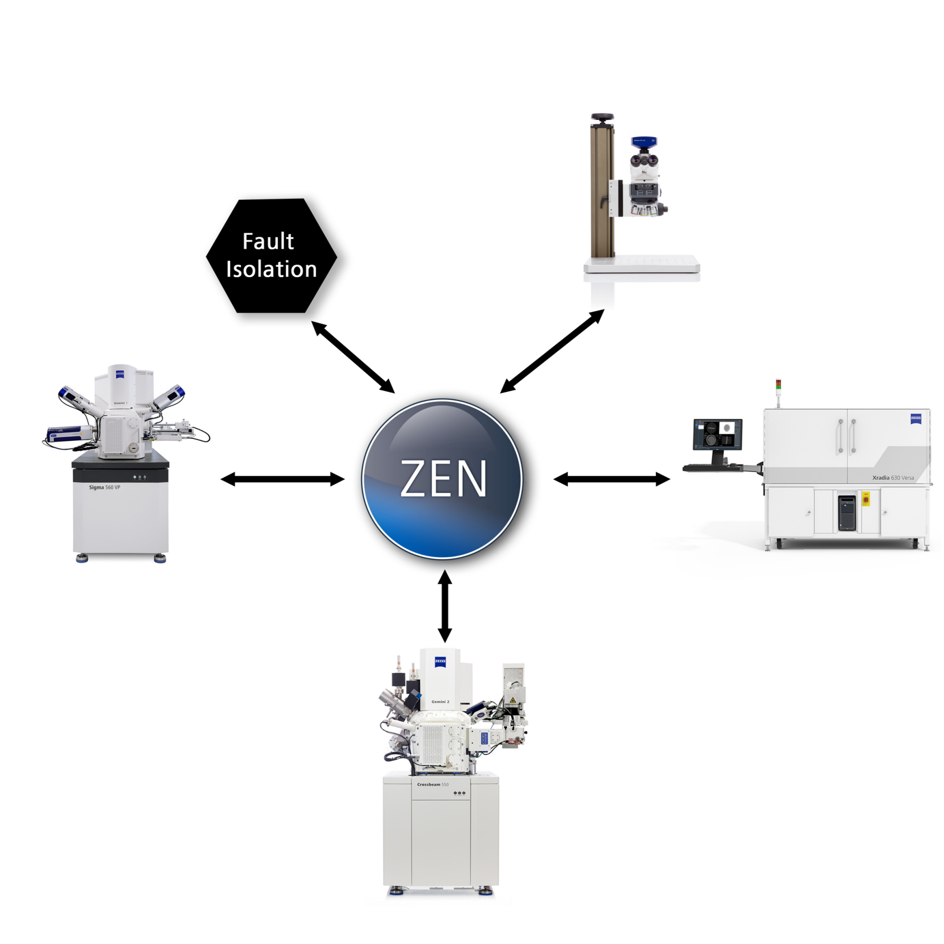

Connected workflows
The semiconductor packaging workflow requires a comprehensive approach to inspection and analysis, involving multiple imaging techniques and data analysis tools.
ZEISS X-ray microscopes can integrate with other microscopy tools and data analysis software and help semiconductor manufacturers to develop connected workflows that streamline and guide the failure analysis, enabling them to identify and take corrective measures to improve yield and reliability more efficiently.
Download the free X-ray microscope failure analysis bundle, what will you receive in your bundle download?
Learn how this technology can be used in this your lab

X-ray microscopy for semiconductor package analysis bundle
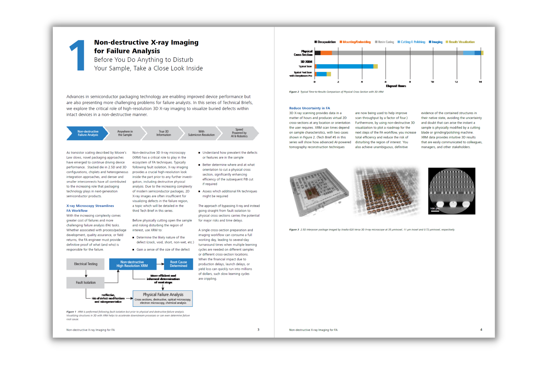
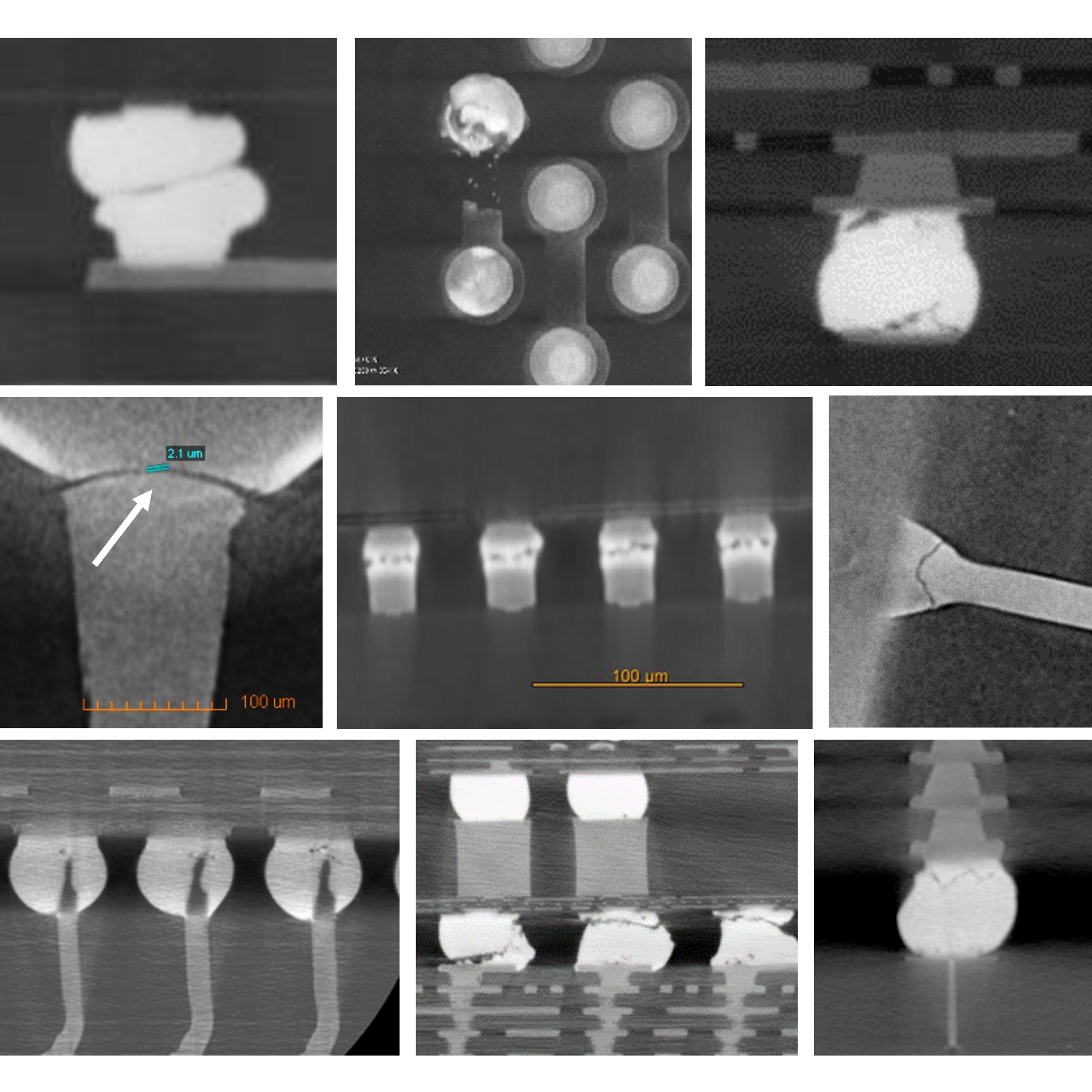
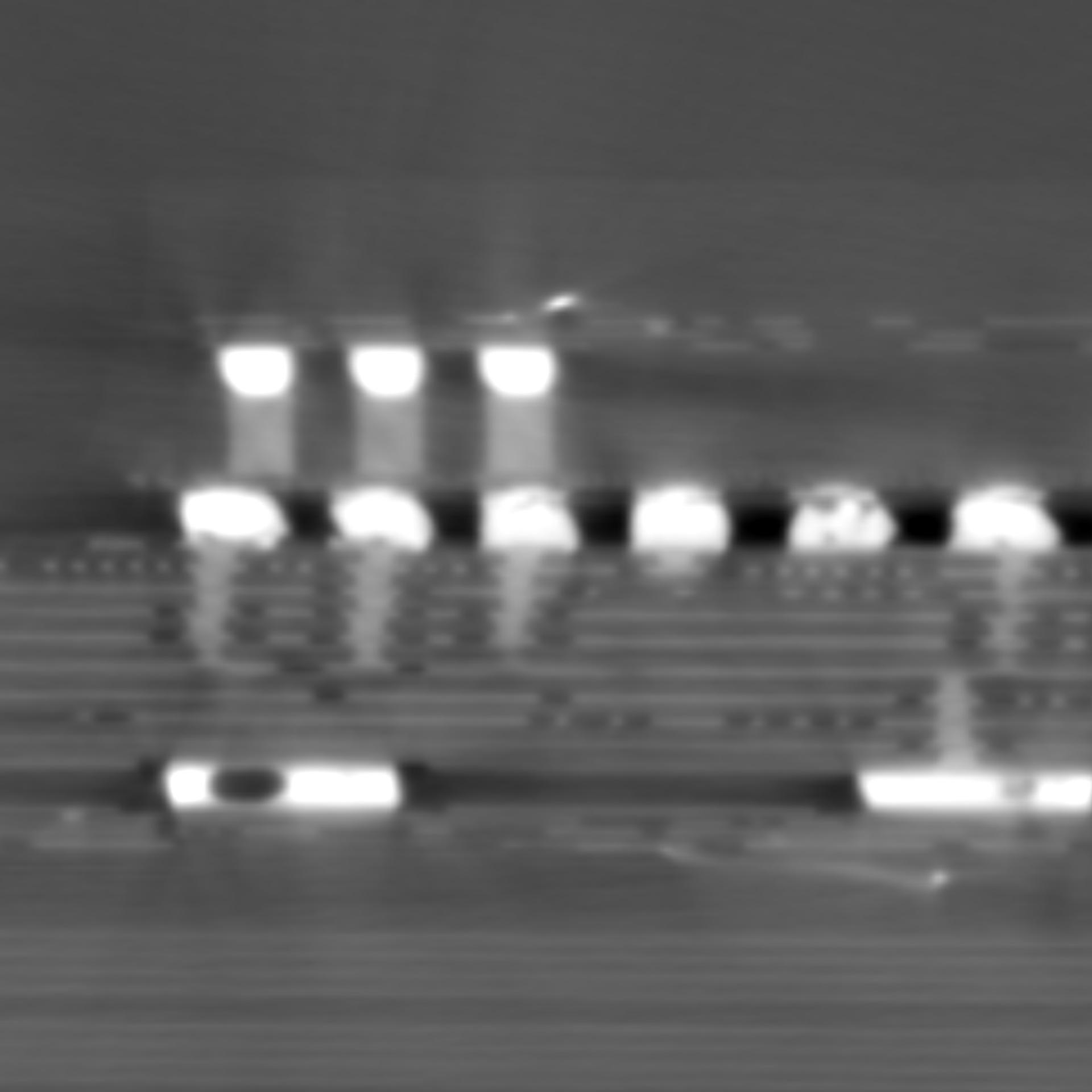
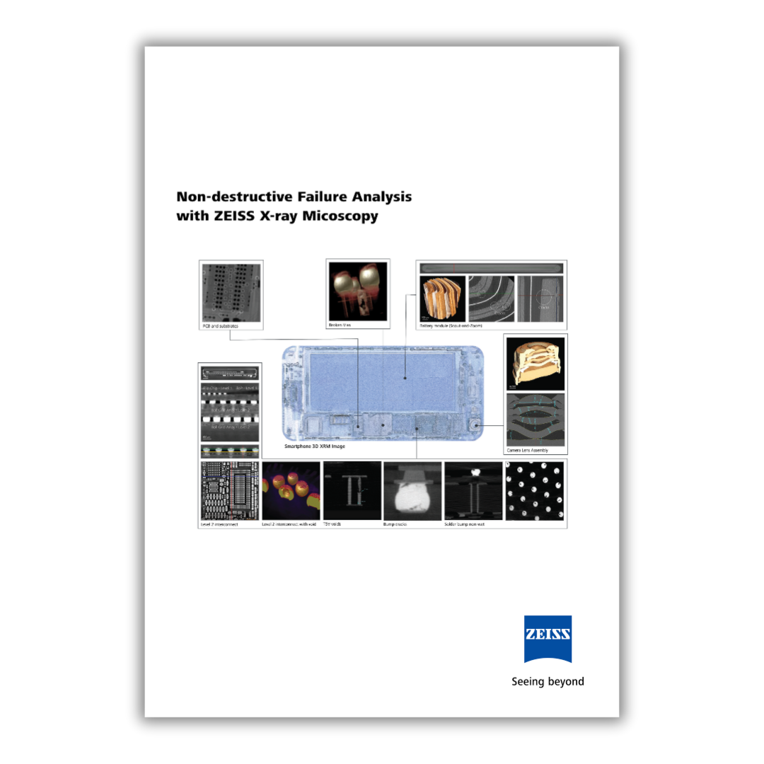
With increasing package complexity comes more challenges for failure analysts to provide definitive proof on the root causes of a failure. Non-destructive 3D X-ray imaging allows visualization inside of disturbing your regions of interest. Acquire high-resolution data in tens of minutes to several hours to increase your FA success rate.
The semiconductor packaging workflow requires a comprehensive approach to inspection and analysis, involving multiple imaging techniques and data analysis tools.
ZEISS X-ray microscopes that can integrate with other microscopy tools and data analysis software can help semiconductor manufacturers to develop connected workflows that streamline the imaging process and facilitate data analysis, enabling them to identify and address defects more efficiently.
Learn how 3D X-ray microscopy fits into your failure analysis workflow and see the throughput benefits as compared to physical cross-sections.

Non-destructive failure analysis for semiconductor packaging
Discover the future of non-destructive failure analysis in the semiconductor industry.
Learn about cutting-edge X-ray microscopy techniques, advanced 40X-P objective lenses, and the revolutionary deep learning high-resolution reconstruction (DLHRR) method.
Enhance your imaging capabilities, speed up data acquisition, and improve fault detection in complex IC packages.