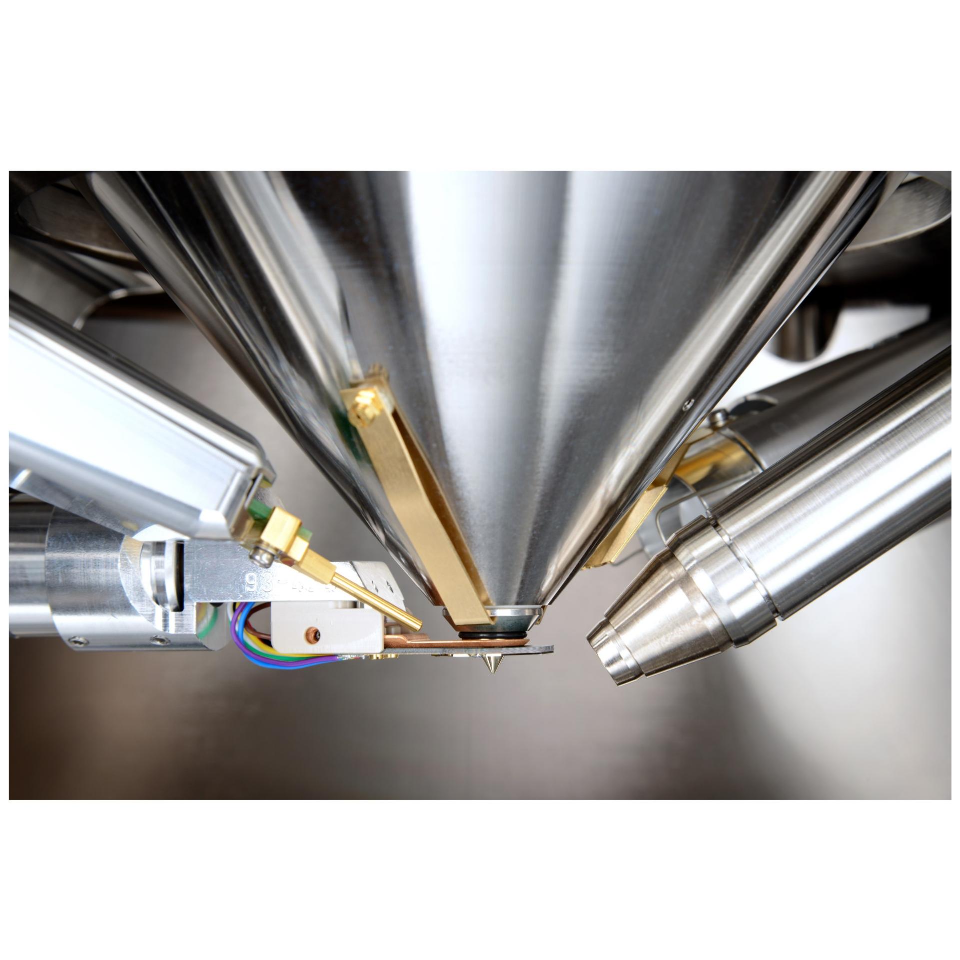
ZEISS FE-SEM
Improving insights in semiconductor package analysisAs packages transition towards three-dimensional architectures, with decreasing interconnect size and increasing material complexity, the development and analysis of processes face significant challenges.
The ZEISS FE-SEM family offers failure analysis techniques that support the complexity of next-generation devices, along with resolution enhancements to align with these advancements.
Learn how MCS Labs uses ZEISS FE-SEM for failure forensics
Distortion free large field of view high pixel resolution imaging
Using ZEISS's FE-SEM Gemini optics for enhanced imagingCombining a high pixel resolution up to 32K x 24K allows imaging of fine details while maintaining the overview and context of the region of interest.
The Gemini optics provide excellent low voltage imaging without immersion optics or stage bias, essential to image non-conductive and beam-sensitive soft polymer materials in advanced packaging.

Enhanced detectors for
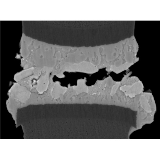
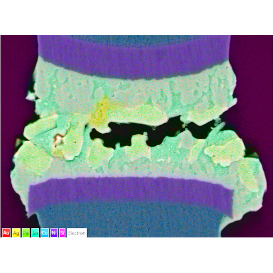
Unmatched material and phase contrastWhether examining Through-Silicon Vias (TSV), Cu-Cu bonds, solder materials, Intermetallic Compound (IMC) layers, or wire bonds, the Gemini column with improved detectors deliver unparalleled imaging performance.
Exceptional material phase and channelling contrast, providing insights for failure analysis and process characterization is routinely achieved.
Unmatched stability and ease of use
Keep your images in perfect focus while switching acceleration voltagesZEISS FE-SEMs are designed to effortlessly maintain focus even while adjusting acceleration voltages. This uncut video demonstrates the seamless transition from 15 kV to 20 V, revealing a consistently sharp and focused image without the need for manual alignment or adjustment, apart from brightness and contrast.
This not only ensures consistent focus but also streamlines your workflow, reducing cycle time and effort required for capturing high-quality images unlocking new levels of efficiency and productivity.

Beam sleeve and VP Mode for high-resolution imaging
Accurate EDS analysis on soft and nonconductive samplesZEISS FE-SEM incorporates a beam sleeve and Variable Pressure (VP) imaging mode to enhance the resolution and analysis of non-conductive and soft materials without extensive sample preparation.
The beam sleeve minimizes the beam path through the low vacuum region, improving signal to noise for high resolution imaging and Energy-Dispersive X-ray Spectroscopy (EDS) analysis further reducing charging effects, and beam-induced damage.
Montage imaging and correlative workflow
For automated ROI acquisitionLarge area imaging workflows are greatly facilitated by ZEISS FE-SEM's recipe-based automated image acquisition, streamlining and automating the imaging process across multiple regions of interest (ROI) and samples.
This powerful feature eliminates the need for manual intervention and enables efficient imaging over large areas. Additionally, the ZEISS correlative workflow allows for the seamless combination of data acquired from multiple modalities and different tools such as light microscopy, 2D X-ray and others, guiding acquisition of specific regions of interest.
A comprehensive understanding of the samples is obtained by integrating data across different imaging techniques, leading to more accurate analysis and insightful results.


Large chamber with ports, optimized geometry for EDS
and immersion-free optics for EBSDThe large chamber is optimized with multiple ports for 180 deg EDS acquisition and EBSD analysis. The fast switching between low current and high current modes in the Gemini column and the immersion-free optics makes it easy to use and without artefacts for analytical work.


Download the correlative workflow for nanoscale failure analysis bundle
For advanced electronics packagesDiscover a groundbreaking correlative workflow that revolutionizes semiconductor defect analysis! Delve into cutting-edge 3D X-ray microscopy (XRM) techniques for non-destructive imaging and precise navigation of nanoscale structures.
Unveil the true potential of advanced package architectures as you eliminate the risk of missing or destroying fault regions in physical failure analysis (PFA) workflows. Enhance your expertise with a proprietary micromachining process that prepares deformation-free surfaces for high-resolution scanning electron microscopy (SEM) analysis.
Stay ahead of the curve and optimize your semiconductor manufacturing processes with this transformative, must-read research!