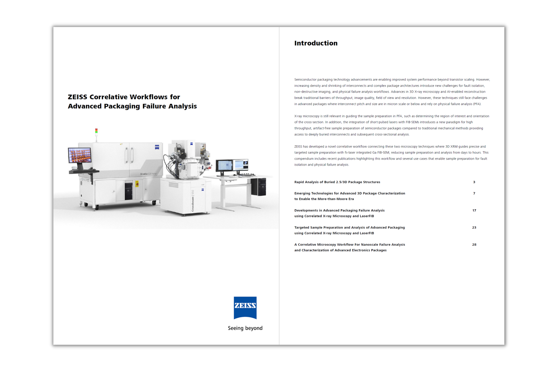
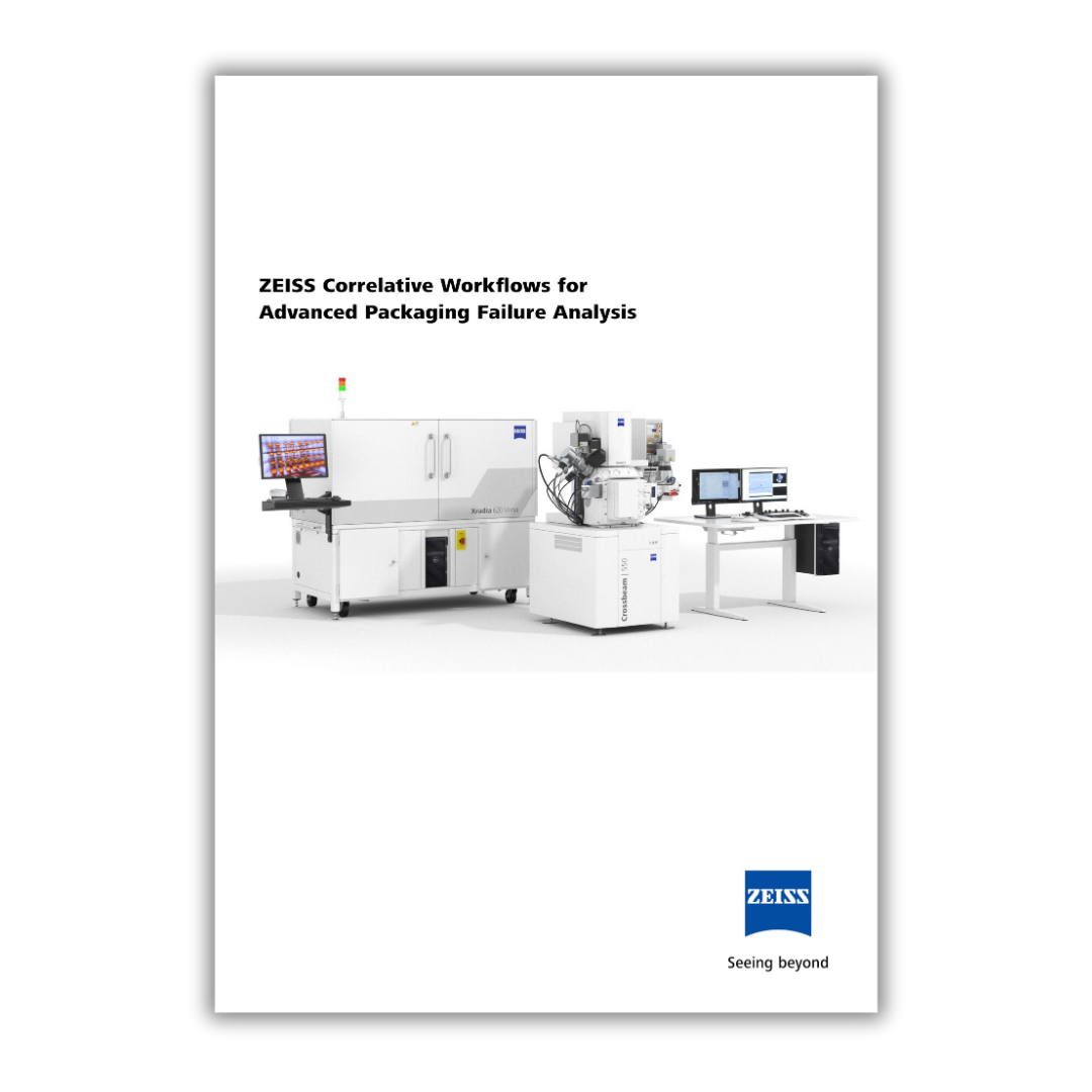
ZEISS Crossbeam Laser
FIB-SEM for high throughput sample preparation and nanoscale imagingParallel advances in FIB-SEM and ultra-fast lasers have radically changed sample preparation, characterization and failure analysis of semiconductor devices and packages.


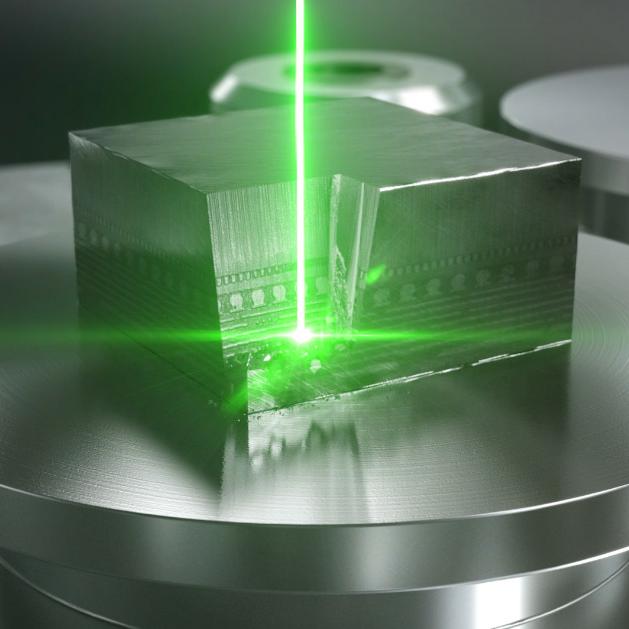

Ultrafast laser-enhanced material removal
For Efficient Sample PreparationAddition of a femtosecond laser to the ZEISS Crossbeam FIB-SEM improves the material removal rates up to 15 mio µm³ per second.
Sample preparation is efficient with minimal heat-affected zone due to the ultrashort pulse duration of the femtosecond laser.
This reduces sample preparation from hours or days to minutes without any artifacts. The laser preparation is suitable for several materials including silicon carbide and glass.
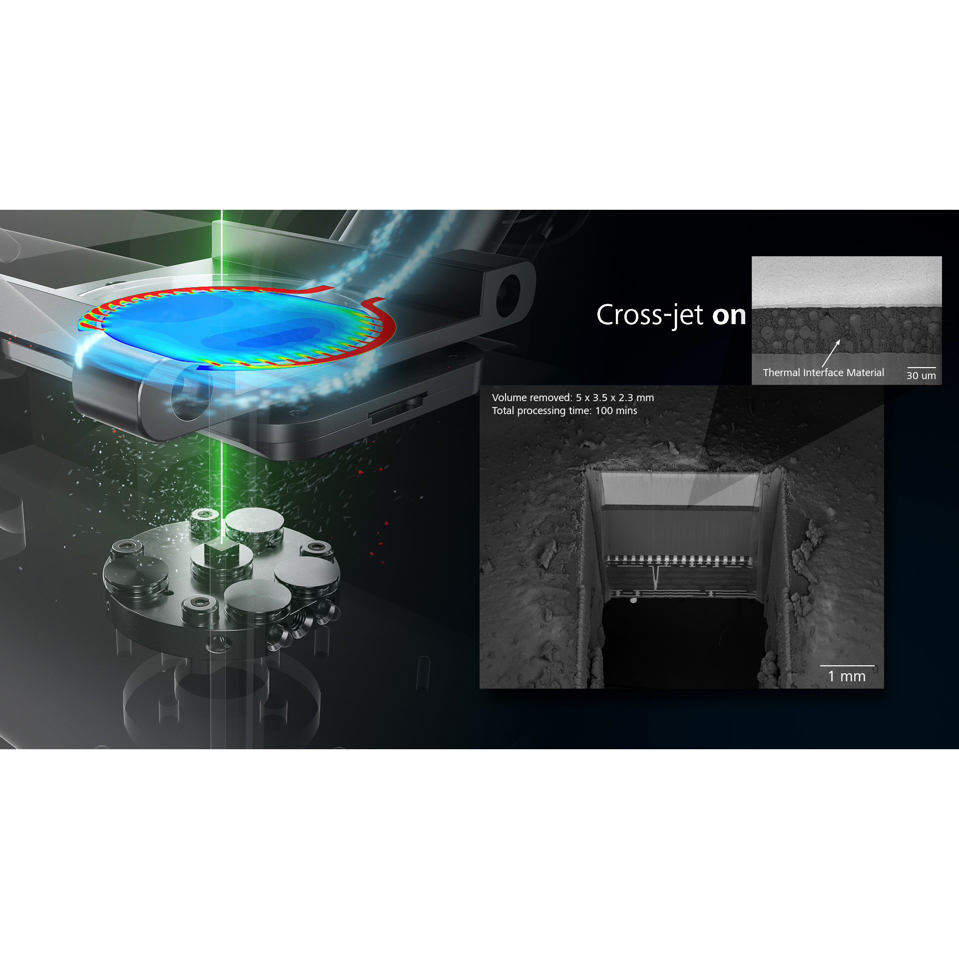

Large volume and contamination free milling
with isolated laser chamber and Cross-JetAccessing structures buried millimetres deep in the package and removal of several cubic mm is now routinely feasible enabling large cross-sections of the entire capacitors, TIM interface through the metal lid, etc
An isolated laser chamber segregates ablation contaminants from the main imaging chamber, maintaining the highest-resolution imaging capability while keeping maintenance costs low.
The new cross-jet, a gas flow of either nitrogen or argon, prevents ablated material to deposit on the protective glass. This enables continuous working for several hours while maintaining consistent laser power and ablation rates.

Automation for precision and productivity
Targeting multiple ROIs and cross-section preparationAutomated shuttling and laser processing in a separate chamber lets you save time and increase throughput, whilst scripting enables automated workflow creation, boosting efficiency in your experiments.
Targeting multiple ROIs and preparation of cross-sections, H-bars, TEM lamella preparation and Atom Probe tomography samples can be automated.

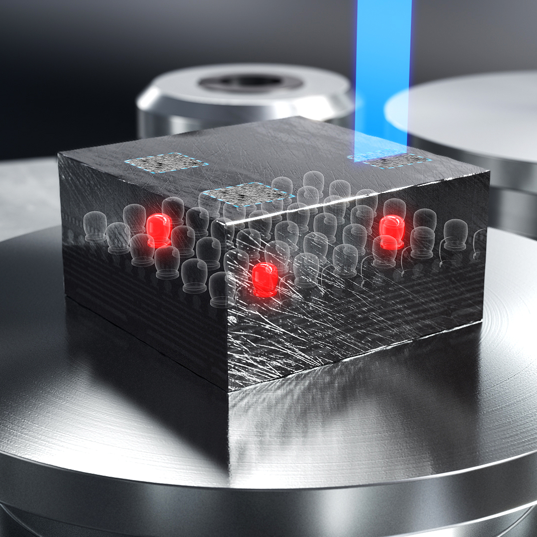
Achieve micron scale precision
With ZEISS Crossbeam LaserZEISS Crossbeam laser tools utilize calibrated laser positioning in a separate chamber to achieve precise targeted sample preparation.
When combined with 3D X-ray data and surface feature registration using SEM imaging in the main chamber, targeting surface and hidden defects deeply buried in the semiconductor package can be routinely achieved with an accuracy better than 2 microns. This enables high throughput targeted sample preparation compared to other conventional techniques
Further enhance your productivity
With X-ray guided connected workflow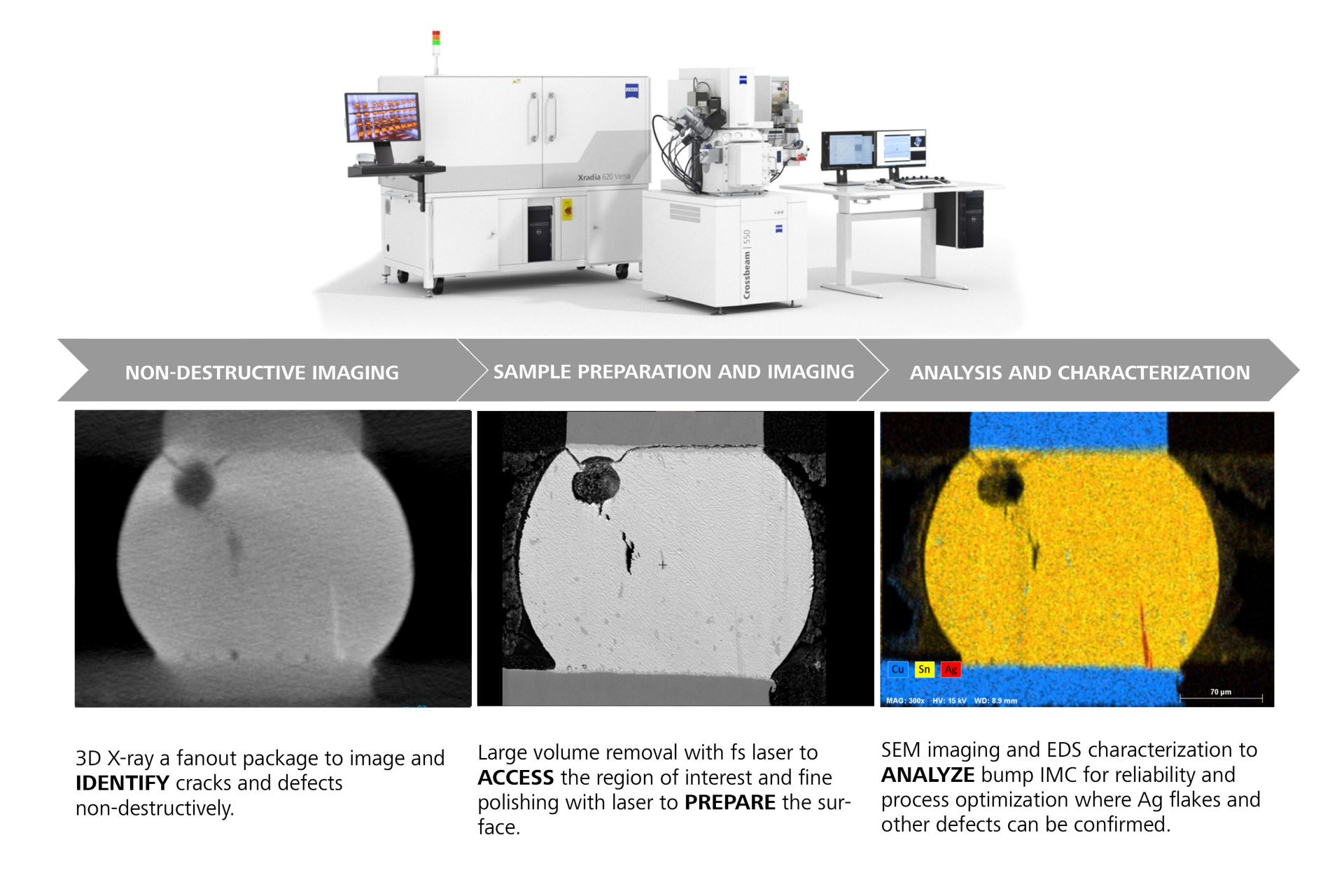

Discover workflows on ZEISS Crossbeam Laser
Explore how guided workflows help you to tailor Laser, TEM Lamella preparation and correlated Cryo workflowsZEISS Crossbeam Laser workflow
Rapidly access deeply buried regions of interest, execute correlated workflows across multiple length scales and acquire better sample representativity with large-volume analysis. Perform 3D imaging and analytics e.g. EDS or EBSD. Now, semi-automated devices enable you to save time and increase your throughput even more.
Add a femtosecond laser to your ZEISS Crossbeam Laser and benefit from site-specific, ultra-fast sample preparation. Keep your FIB-SEM chamber clean and operate the system remotely with a semi-automated workflow when needed.
Your benefits:
- Gain rapid access to deeply buried structures
- Benefit from minimal damage and heat affected zones due to femtosecond laser pulses in a controlled vacuum environment
- Perform laser work in a dedicated integrated chamber to maintain cleanliness of your FIB-SEM main chamber and detectors
- Automate laser processing, polishing, cleaning and transfer of the sample to the FIB chamber
- Prepare multiple samples from cross-sections over TEM lamellae to pillar arrays, and work efficiently by using pre-installed recipes for different materials

Download the correlative workflows for advanced packaging failure analysis
For efficient sample preparationAddition of a femtosecond laser to the ZEISS Crossbeam FIB-SEM improves the material removal rates up to 15 mio µm³ per second.
Sample preparation is efficient with minimal heat-affected zone due to the ultrashort pulse duration of the femtosecond laser.
This reduces sample preparation from hours or days to minutes without any artifacts. The laser preparation is suitable for several materials including silicon carbide and glass.