
Advancing Microscopy & Imaging Technologies
Join ZEISS, Kleindiek, and industry experts for insights on AI-driven microscopy, 3D X-ray imaging, FIB-SEM, and FESEM nanoprobing.- 00 years
- 00 months
- 00 days
- 00 hours
- 00 minutes
- 00 seconds
Agenda
|
9.00am - 9.30am |
Breakfast |
|---|---|
|
9.30am - 10.15am |
Opening |
|
10.15am - 11.15am |
AI in Microscopy: AI-supported solutions that simplify analysis |
|
11.15am - 12.30pm |
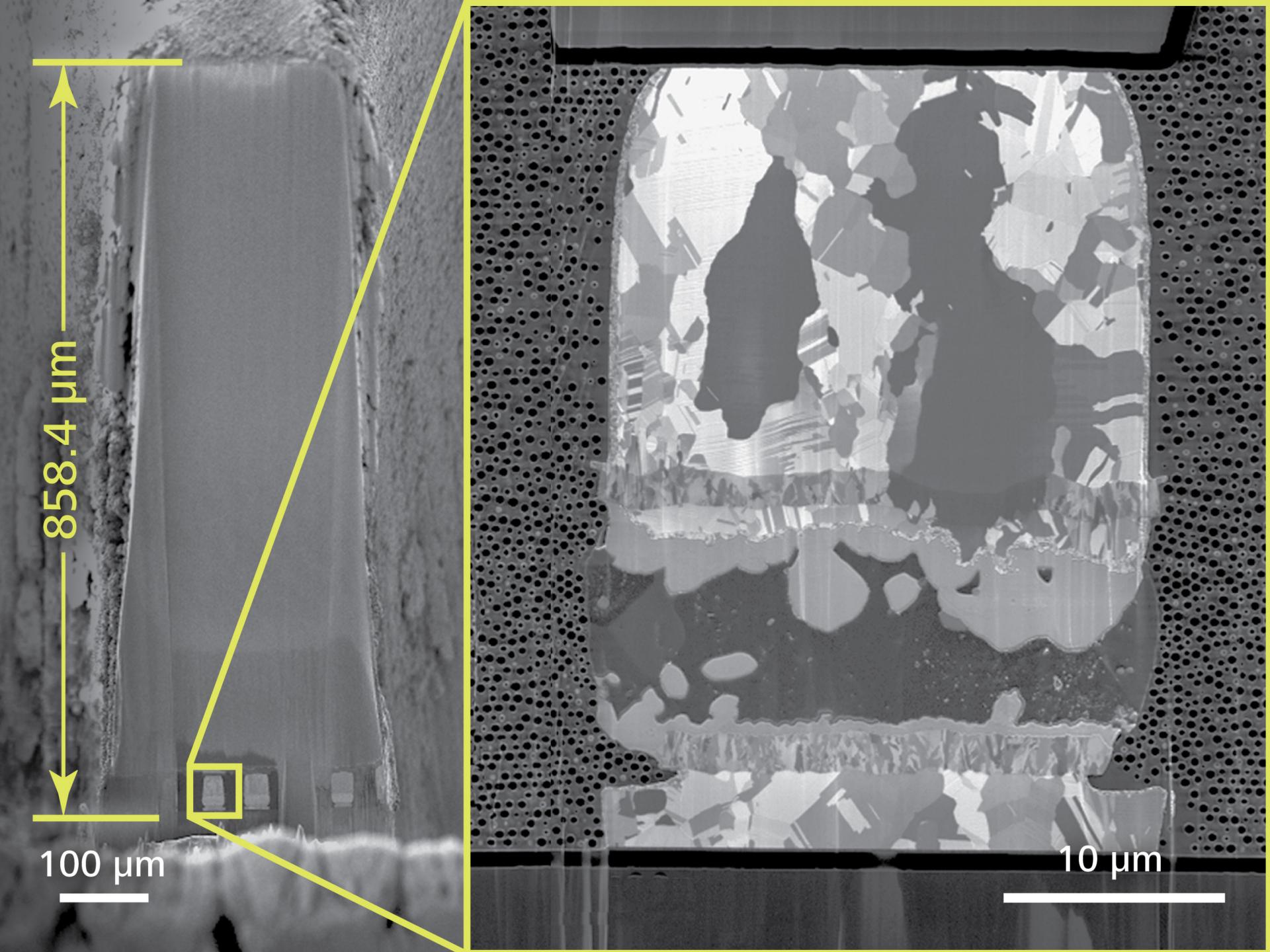
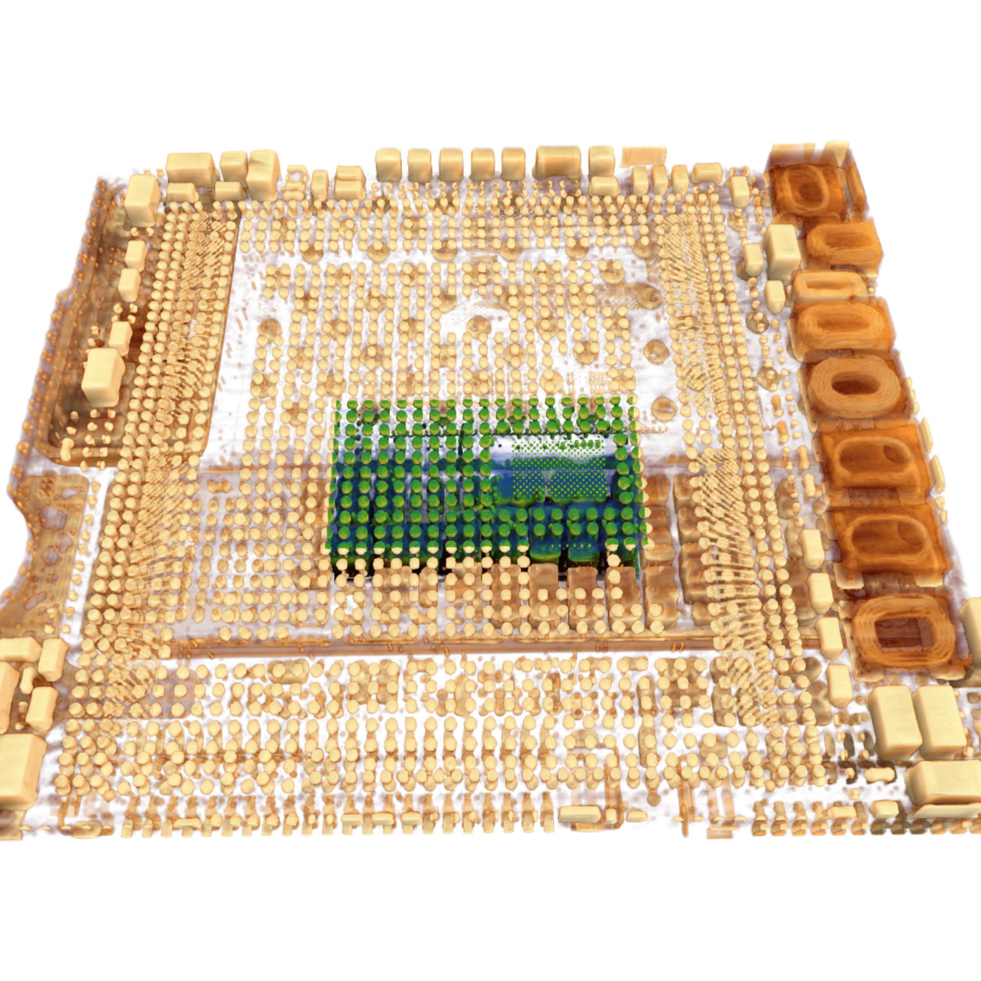
The next generation ZEISS Versa 3D XRM with AI Powered Imaging Solution for Semiconductor Package Structural Analysis and Correlative Microscopic Failure Analysis Virtual Live Demo of ZEISS Versa 3D XRM |
|
12.30pm - 1.45pm |
Lunch |
|
1.45pm - 3.15pm |
Slot 1: Overcoming Bottlenecks in Manual TEM Sample Preparation Slot 2: ZEISS Samplefab: TEM sample preparation success rates, Guaranteed! Slot 3: Accessing the Inaccessible: Overcoming Packaging Failure Analysis Challenges with Laser-FIB Workflows |
|
3.15pm - 3.45pm |
Tea Break |
|
3.45pm - 4.45pm |
Addressing Nanoprobing Challenges for the Most Recent Technology Nodes |
|
4.45pm - 5.00pm |
Closing |