
Exploring Defects & Structures: Microscopy Solutions for Advanced Semiconductor Packaging
Discover cutting-edge imaging and characterization solutions with NUS SHINE and ZEISS.- 00 years
- 00 months
- 00 days
- 00 hours
- 00 minutes
- 00 seconds
Agenda
-
1:30 PM - 2:00 PM
Registration
2:00 PM - 2:15 PM
Opening Address – Prof Lim Yeow Kheng, Programme Director, NUS SHINE
2:15 PM - 2:45 PM
Non-Destructive 3D Imaging and AI-driven Deep Learning for Semiconductor Materials – Dr Sky Xie
2:45 PM - 3:15 PM
Advancing Electronic Digital Twins with X-Ray Imaging and Machine Learning – ZhanSen Shi, NUS SHINE
3:15 PM - 3:45 PM
Tea Break
3:45 PM - 4:15 PM
Implementing ML in X-ray CT for Effective Failure Analysis – Dr. Riko I Made, Institute of Materials Research and
Engineering, A*STAR
4:15 PM - 4:45 PM
Correlative Microscopy Workflow for Targeted Subsurface Semiconductor Materials Research - Dr Feng Lin Ng
4:45 PM - 5:00 PM
Closing Address + Quiz
-
Dr. Sky Xie – ZEISS
Senior Regional Product and Application Sales Specialist, Research Microscopy SolutionsDr. Sky Xie earned his B.Eng. (Honors) from Nanyang Technological University (NTU) and later completed a Ph.D. in Materials Science and Engineering. He has extensive experience in nanostructured metallic, ceramic, and composite materials, previously working as a Research Scientist at NTU. Since 2017, he has specialized in X-ray Microscopy, Electron Microscopy, and Light Microscopy at ZEISS.
Presentation
Non-Destructive 3D Imaging and AI-driven Deep Learning for Semiconductor Materials
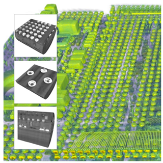
X-ray Computed Tomography (CT) enables non-destructive analysis of internal semiconductor microstructures, crucial for failure analysis (FA). ZEISS’ X-ray Microscopes (XRM) use synchrotron technology to capture high-resolution 3D images, detecting buried defects at sub-micron scales. Deep-learning reconstruction enhances imaging efficiency, reducing acquisition time while preserving crucial defect details. This approach outperforms conventional techniques, improving signal extraction from low-dose data for advanced failure analysis.
Mr. Shi Zhansen - NUS SHINE
Shi Zhansen is an engineer with a strong background in electrical engineering. He holds both a Bachelor’s and Master’s degree from the National University of Singapore (NUS). With a passion for problem-solving, he enjoys working with data, finding patterns, and developing practical solutions.
Zhansen has experience in design and innovation, allowing him to approach challenges creatively. He works well in teams, collaborating with others to turn ideas into reality. His interest in technology drives him to keep learning and improving.
Committed to making an impact, Zhansen continues to explore new ways to apply his skills in meaningful projects.
Presentation
Advancing Electronic Digital Twins with X-Ray Imaging and Machine Learning
With the increasing complexity of 3D integrated circuits (3D-ICs), failure analysis requires advanced visualization and diagnostic methods. X-ray imaging plays a crucial role in revealing internal structures, enabling more accurate defect detection and analysis. This presentation highlights how X-ray images can enhance machine learning models for reconstructing circuit layouts, identifying defects, and improving electronic digital twin creation. By leveraging publicly available segmentation techniques, we demonstrate how X-ray imaging can contribute to more precise failure analysis and predictive modelling. This approach paves the way for more efficient diagnostics in modern electronics.
Dr. Feng Lin Ng – ZEISS
Business Development Specialist, APAC – Materials Research, Research Microscopy SolutionsDr. Feng Lin Ng received a Ph.D. in Materials Science and Engineering from NTU, specializing in polymeric cell culture systems. She has worked as a Research Scientist at SIMTech, A*STAR, focusing on polymer materials, MedTech, Aerospace, and Sustainability applications. At ZEISS, she leads business development in Electron & X-ray Microscopy for Materials Research.
Presentation
Correlative Microscopy Workflow for Targeted Subsurface Semiconductor Materials ResearchCorrelative microscopy bridges multi-scale imaging for semiconductor research, providing precise subsurface analysis. A comprehensive workflow integrates X-ray imaging and FIB-SEM, enabling targeted failure analysis and materials characterization. This workflow connects macro to sub-nanometer length scales, offering unparalleled insights into semiconductor microstructure-property relationships. Case studies illustrate its impact on device failure analysis and semiconductor materials research.
Dr. Riko I Made - Institute of Materials Research and Engineering (IMRE), Agency for Science, Technology and Research (A*STAR)
ScientistI joined A*STAR – IMRE in 2021 as a Scientist and have been working at the intersection of Materials Science Engineering and Artificial Intelligence. My research focuses on developing and applying advanced machine learning methods to tackle critical challenges in materials processing and characterization. Currently, my work spans several key areas: Process Optimization: Leveraging AI/ML techniques to optimize material processing parameters. The goal is to enhance performance, reduce costs, and improve sustainability. Defect Localization and Characterization: Developing AI-powered algorithms for accurate and efficient detection, localization, and characterization of defects in materials using techniques such as microscopy and tomography. Data-Driven Materials Discovery: Utilizing machine learning to analyze large experimental and simulation datasets, accelerating the discovery of new materials with desired properties. This includes developing predictive models, identifying key material descriptors, and gaining deeper insights into complex material behaviours.
Presentation
Implementing ML in X-ray CT for Effective Failure AnalysisThis workshop explores the transformative potential of machine learning (ML) in microelectronics failure analysis, focusing on techniques that leverage X-ray Computed Tomography (CT). We'll begin by reviewing the current state-of-the-art, showcasing successful applications and prevalent ML-driven approaches for X-ray CT failure analysis. This includes examining how ML automates defect detection, segmentation, and classification, along with a discussion of the benefits and limitations of these methods.
Building on this foundation, we'll explore exciting opportunities and future directions for ML in this field. We'll delve into potential advancements such as 3D image analysis, automated root cause analysis, predictive failure modeling, and integration with other analytical techniques. Critically, we'll also address the challenges hindering wider adoption, including data requirements, computational resources, and the need for robust and explainable AI models.
Finally, we'll showcase ongoing research from our group, demonstrating practical applications of ML to real-world microelectronics failure analysis problems using X-ray CT. We'll share our findings, discuss our methodologies, and highlight the potential impact of this work on improving the efficiency and accuracy of failure analysis. This workshop aims to stimulate discussion and collaboration on the future of ML-driven failure analysis, ultimately contributing to the development and deployment of more reliable and robust microelectronic devices.
Location
National University of Singapore
ZOYC organisers
ZEISS would like to thank the co-organisersRegister
Fill in the form below to secure your spotWhy Attend?
- See real-world XRM results from semiconductor packaging failure analysis
- Gain insights into FIB/SEM correlative workflows
- Connect with leading experts from academia and industry
- Discover opportunities for collaboration
Your work in semiconductor research evolves with better imaging. Are you ready to explore the future of microscopy?


