
Advancing Microscopy & Imaging Technologies
Join ZEISS, and industry experts for insights on AI-driven microscopy, 3D X-ray imaging, FIB-SEM, and more.- 00 years
- 00 months
- 00 days
- 00 hours
- 00 minutes
- 00 seconds
Agenda and Talk Topics
|
9.00am - 9.30am |
Opening |
|---|---|
|
9.30am - 10.00am |
Labless Enable High-Quality Development of Singapore Semiconductor |
|
10.00am - 10.50am |
AI in Microscopy: AI-supported solutions that simplify analysis |
|
10.50am - 11.00am |
Break |
|
11.00am - 12.00pm |
Defect localization and device characterization in the electron microscope |
|
12.00pm - 1.00pm |
Lunch |
|
1.00pm - 1.45pm |
Overcoming Bottlenecks in Manual TEM Sample Preparation |
|
1.45pm - 2.15pm |
ZEISS Samplefab: TEM sample preparation success rates, Guaranteed! |
|
2.15pm - 3.15pm |
Blockwise: Transforming Microscope Automation |
|
3.15pm - 3.30pm |
Tea Break |
|
3.30pm - 4.30pm |
Discover new insights for package failure analysis with X-ray Microscopy |
|
4.30pm - 5.00pm |
Streamlining Package Failure Analysis: A Correlative Workflow Approach |
|
5.00pm - 5.30pm |
Advanced SEM-EDS-EBSD-Raman Techniques for Semiconductor Inspection and Metrology |
|
5.30pm - 5.45pm |
Quiz and Closing |

Singapore Semiconductor industry facing challenges in high investments in high-end equipment, limited specialized technical expertise, diversify technological iteration, which often limit the company to achieve optimal R&D performance. Wintech Nano's LABLESS Model exemplifies an innovative paradigm of specialized segmentation in the semiconductor industry, centering on the outsourcing of "essential non-core" R&D testing processes to third-party laboratories. By this means, enterprises are enabled to access impartial, high-efficiency services—including failure analysis, material characterization, and process monitoring—without establishing full-scale in-house labs, with costs reduced by over 60%.
Wintech Nano, which operates "Super Laboratory" in Singapore, Suzhou and other locations. Over 2,000 global clients across the semiconductor value chain—from IC design, Wafer Fab, Packaging and Material sectors. While a transitional "Lab-Lite" model (combining small in-house labs with outsourcing) is currently employed by the industry, testing has been established as an independent sector by LABLESS. Driven by technological innovation, traditional R&D barriers are dismantled by LABLESS model, and a collaborative ecosystem that accelerates innovation and enhances operational efficiency across the Singapore semiconductor industry.


In our daily testing, we generate a large number of images. How can we use these images to quickly and effectively obtain statistical data, and even predict product quality? Zen Core software offers this possibilities. Traditional segmentation, machine learning and deep natural network (DNN) learning can support image processing and analysis. At the same time, Zen Core software can perform batch processing and reduce the time for data statistics and reporting to improve the productivity and efficiency.


The electron microscope can take interesting pictures of your devices. Its real power, however, for semiconductor device engineering and yield management, is seen in the interactions of the electron beam with the electrical properties of your device. This talk will cover various techniques at the disposal of the GeminiSEM. Nanoprobing can not only interrogate electrical properties of individual devices but also image the depletion zones of p/n junctions. Passive Voltage Contrast can find opens in nets as well as provide information on junction health across a wide field of view. Tomographic, AFM-in-SEM analysis can show layer-by-layer device information while milling. Electron Channeling Contrast Imaging finds crystal defects. Questions and followup meetings are welcome.


TEM sample preparation remains a critical task for semiconductor failure analysis and characterization, requiring precision, throughput, and quality. This session will focus on how ZEISS Crossbeam enables customers to navigate common challenges in TEM sample preparation while achieving greater efficiency and higher success rates in demanding workflows.


ZEISS Samplefab provides a fully automated solution for high-throughput, multi-site TEM sample preparation, delivering high lamella success rates with minimal user effort. This session will cover how its pre-configured FIB-SEM system, reliable automation, and easy-to-use interface help semiconductor labs improve efficiency, productivity, and repeatability.


Blockwise is an innovative, user-friendly software tool designed to automate microscope control, image analysis, and metrology tasks, addressing the growing demand for electron microscopy (EM) automation in the electronics sector. Combining ease of use with powerful automation capabilities, Blockwise enables customers to perform complex microscopy tasks with minimal programming knowledge through its intuitive drag-and-drop interface. Initially focused on FESEM automation, Blockwise will expand to support FIB and LM. The integration of AI-based feature, defect, and anomaly detection enhances usability and precision. Custom services from the Solutions Lab, including workflow development, custom block creation, and bespoke training programs, ensure customers can fully leverage Blockwise's capabilities to meet their unique needs.


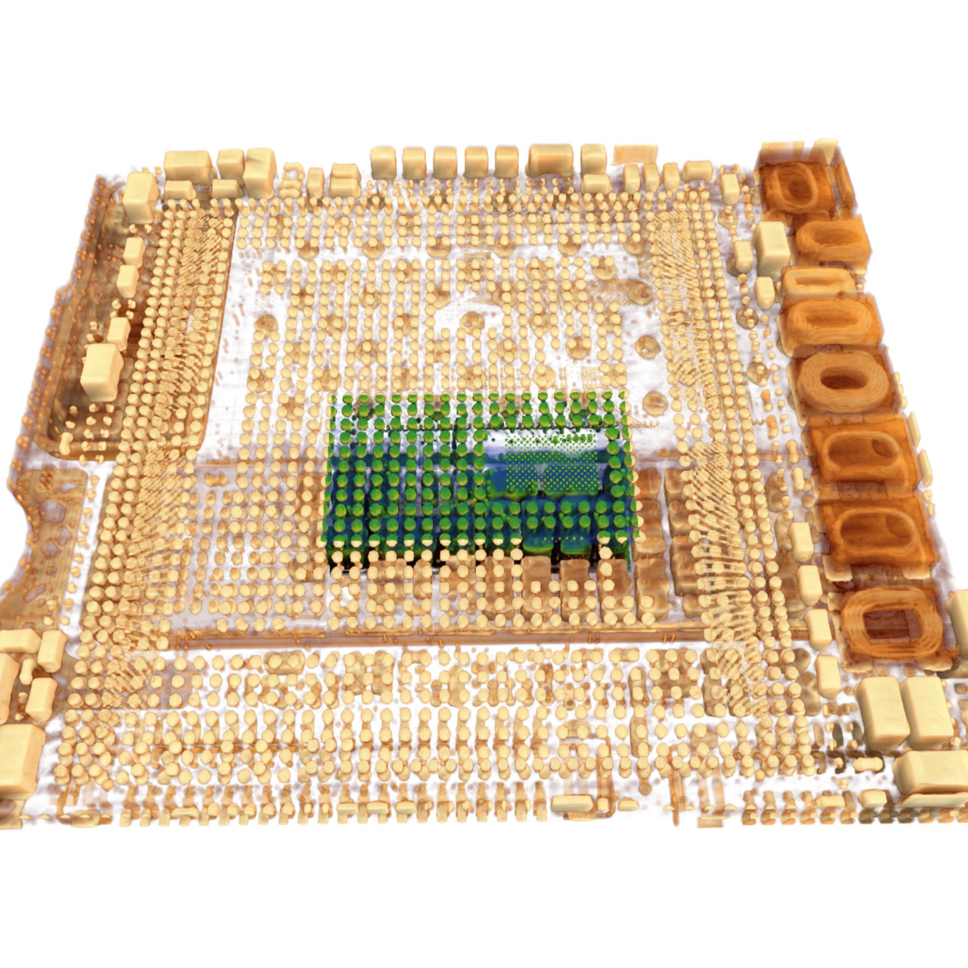
3D X-ray microscopes (XRM) has been widely adopted in package level failure analysis over the past decade. However, the non-destructive imaging technique is challenged as packaging innovations rapidly emerge. We will present most recent progress on XRM resolution improvement, scan acceleration, AI-based reconstructions and correlative microscopic workflows with use case studies included. A new 50 nm resolution nanotomography technique, recently powered by a deep learning reconstruction method will be also briefly reported.


Detecting and analyzing rare micron-sized defects or anomalous particles buried deep within semiconductor packages presents a significant challenge, particularly when these flaws are hidden within a largely homogeneous material matrix. This session explores how a correlative workflow can enable efficient and accurate identification and analysis of such defects. The approach combines non-destructive 3D X-ray microscopy (XRM) for precise localization of subsurface anomalies with advanced focused ion beam scanning electron microscopy (FIB-SEM) equipped with an integrated femtosecond (fs) laser.


Failure analysis of semiconductor devices plays an important role for improving product quality and advancing semiconductor processing technology. However, these failures are often complex, occurring across a wide range of spatial scales, from a few nanometers to tens of microns. This complexity necessitates structural inspection and measurement at various scales. Many issues also arise from material interactions, particularly in microstructures containing elements like Al, Cu, Sn, and Ni, which can form intermetallic compounds. Additionally, identifying embedded contaminants is a routine task. Advanced SEM-based analysis tools are essential for these tasks, as they can measure and analyze complex microstructures, identify materials and contaminants, and analyze material crystalline changes. This information is useful for process improvement and quality control.
This presentation will introduce the latest EDS, EBSD, and Raman technologies on the SEM platform as well as their applications. Analysis cases for various semiconductor devices include:
1. High-resolution elemental mapping of DRAM, flash memory devices, GaN, and SiC devices for structural and contamination inspection.
2. Material analysis in solder bumps, interconnects, and flash memory devices.
3. Measurement of GaN and SiC single crystals.