
ZEISS at SEMICON 2024
Booth #901- 00 years
- 00 months
- 00 days
- 00 hours
- 00 minutes
- 00 seconds
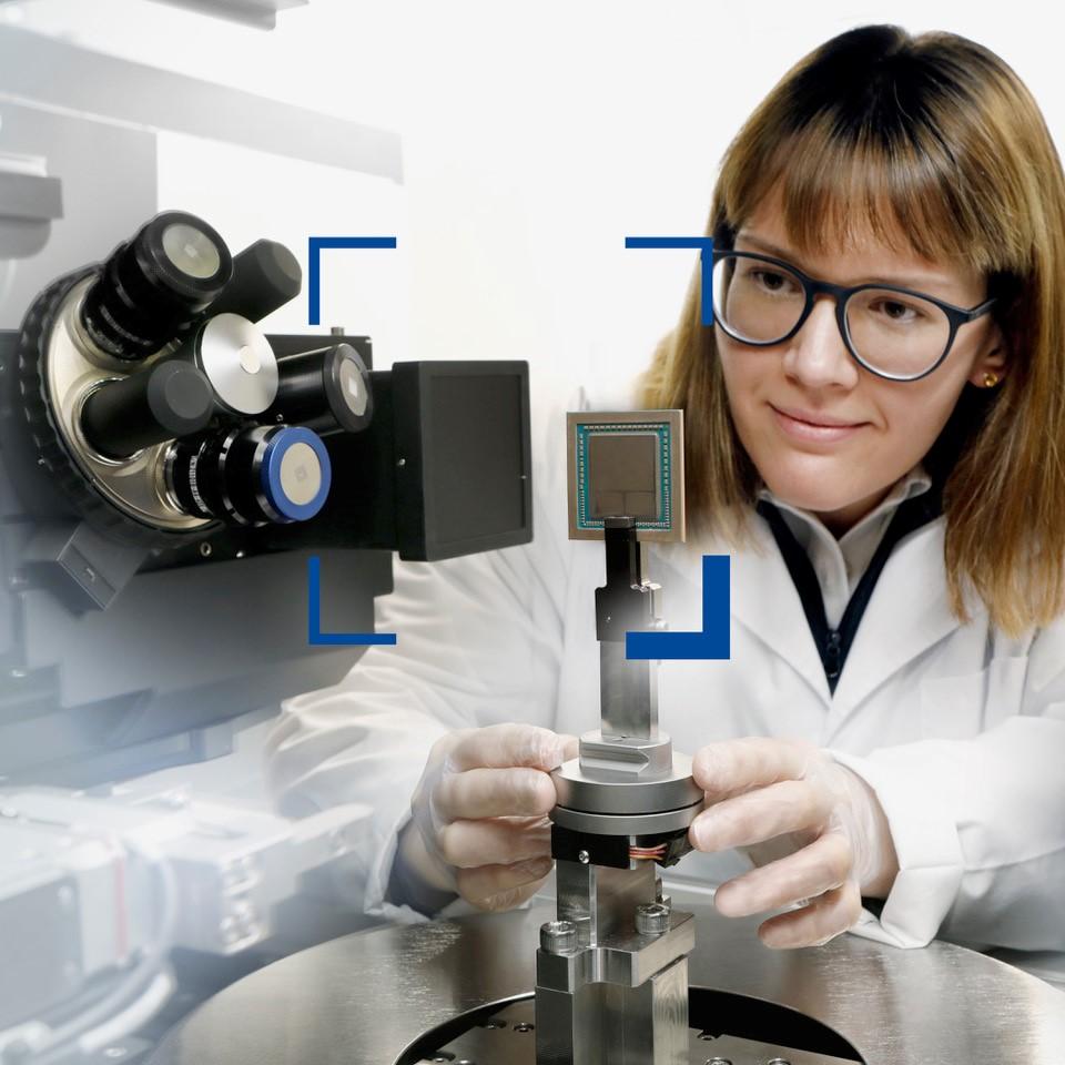
Improve Your FA for Power Semiconductor and Advanced Devices
New materials and semiconductor technologies are advancing the performance of next-generation electronics. Fast and accurate failure analysis becomes more important than ever for all product life cycle stages – from R&D to yield improvement to field returns. ZEISS offers advanced 2D and 3D imaging solutions for front-end and back-end processes. Please visit booth #A8 at IPFA to speak with our team about our unique X-ray, FE-SEM and FIB-SEM microscopy solutions for failure analysis and process development.
Discover how GeminiSEM FE-SEM enables ultra-low voltage surface imaging and large field-of-view nanoprobing for your most demanding imaging and analytical tasks. See how Xradia 3D X-ray microscopes powered by artificial intelligence deliver faster scan times with images that look better than ever. Explore how Crossbeam FIB-SEM achieves single-digit-nm 3D resolution for failure analysis, constructional analysis, or metrology of the smallest logic and memory structures. Learn about our breakthrough Crossbeam laser FIB-SEM for rapid nanoscale imaging of deeply buried features in stacked die and packages and high-resolution real-time SEM control for lamella preparation.


ZEISS Microscopy Solutions for Failure Analysis


ZEISS Xradia Versa X-ray Microscope
Image buried defects and package structures non-destructively

ZEISS Crossbeam laser FIB-SEM
Rapidly access site-specific features buried deeply within IC packages

ZEISS Crossbeam FIB-SEM
Achieve versatile, efficient imaging and processing for high-resolution 2D and 3D insights
