
Learn how to use ZEISS XRM to improve success rates & efficiency for semiconductor package failure analysis
Visualize in 3D without altering your defectWhile searching for the root cause of problems in your device,
3D X-ray microscopy can help you…
Download the free X-ray microscope failure analysis bundle, what will you receive in your bundle download?
Learn how this technology can be used in this your lab

X-ray microscopy for semiconductor package analysis bundle
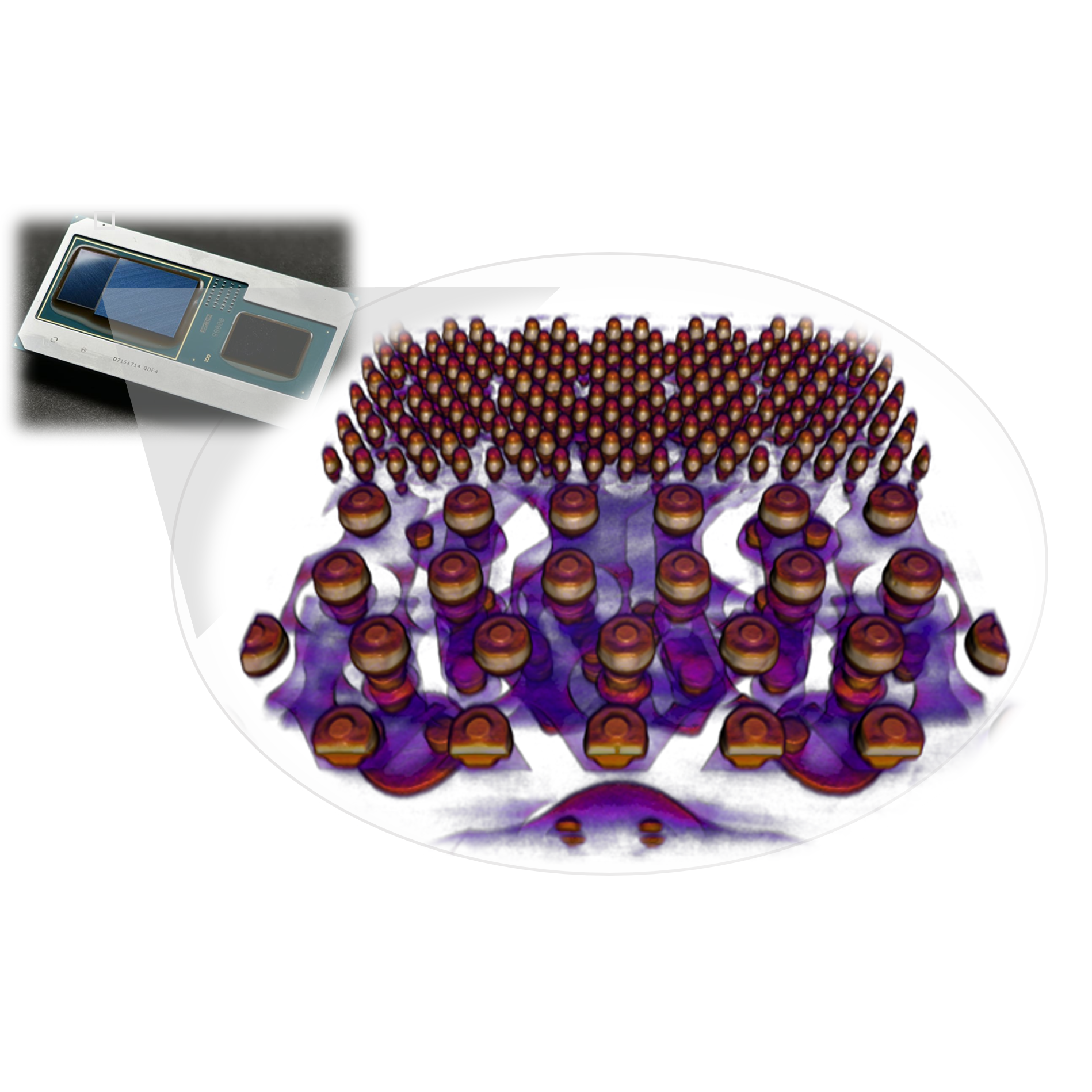
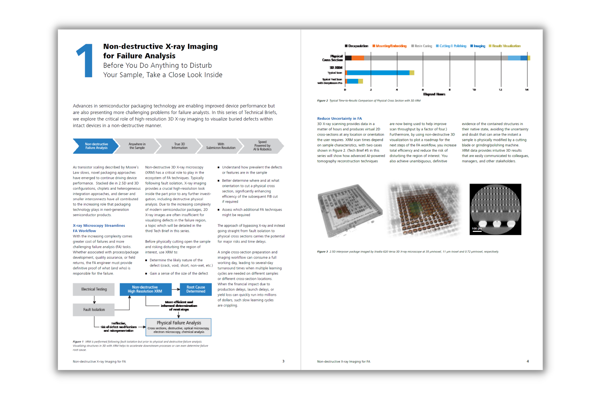
With increasing package complexity comes more challenges for failure analysts to provide definitive proof on the root causes of a failure. Non-destructive 3D X-ray imaging allows visualization inside of disturbing your regions of interest. Acquire high-resolution data in tens of minutes to several hours to increase your FA success rate.
The semiconductor packaging workflow requires a comprehensive approach to inspection and analysis, involving multiple imaging techniques and data analysis tools.
ZEISS X-ray microscopes that can integrate with other microscopy tools and data analysis software can help semiconductor manufacturers to develop connected workflows that streamline the imaging process and facilitate data analysis, enabling them to identify and address defects more efficiently.
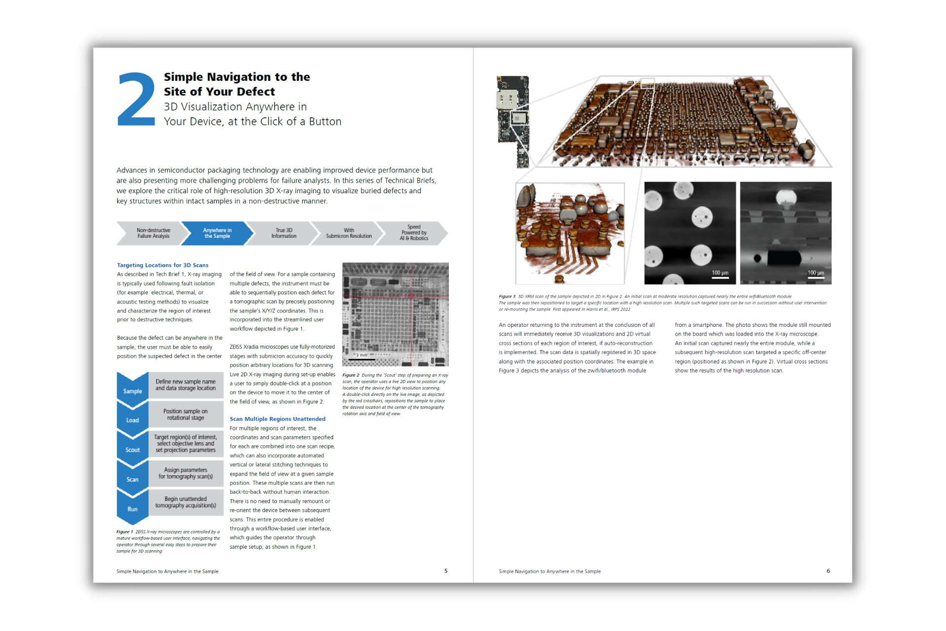
Learn how 3D X-ray microscopy fits into your failure analysis workflow and see the throughput benefits as compared to physical cross-sections.

Non-destructive failure analysis for semiconductor packaging
Discover the future of non-destructive failure analysis in the semiconductor industry.
Learn about cutting-edge X-ray microscopy techniques, advanced 40X-P objective lenses, and the revolutionary deep learning high-resolution reconstruction (DLHRR) method.
Enhance your imaging capabilities, speed up data acquisition, and improve fault detection in complex IC packages.
How the bundle looks like
When you download it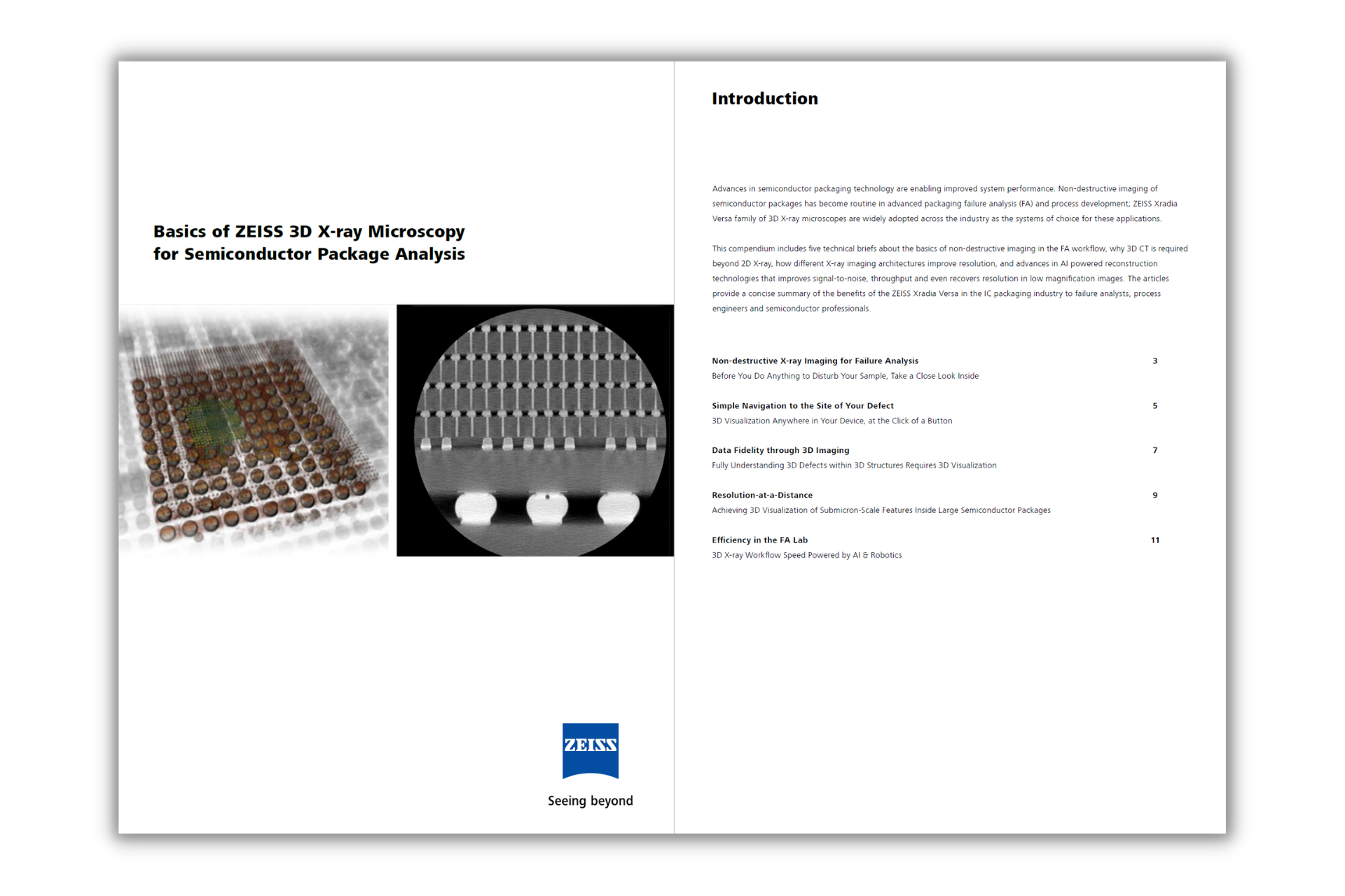


Here is what you will learn after downloading the ZEISS XRM bundles for failure analysis
Here is what you'll learn after downloading this bundle:
1. Learn how to apply advanced failure analysis techniques: Both documents discuss novel techniques for failure analysis in semiconductor manufacturing, including X-ray microscopy (XRM) and wafer-to-wafer bonding analysis. Reading these documents will provide engineers with an understanding of the latest methods and tools for detecting and analyzing failures, which will help them improve their skills and enhance the overall efficiency and effectiveness of failure analysis in their work.
2. Learn how to use deep learning in failure analysis: The second document introduces a deep learning high-resolution reconstruction (DLHRR) method that improves X-ray imaging for failure analysis. Engineers will learn how to implement pre-trained neural networks to speed up data acquisition and improve image quality, which can significantly reduce the time required for data acquisition and improve the quality of failure analysis results.
3. Learn how to tackle challenges in imaging advanced packages: The second document discusses the increasing challenges in imaging advanced semiconductor packages due to more densely packed IC interconnects. Engineers will gain insights into the limitations of current imaging techniques and the need for innovative solutions, helping them identify areas for improvement and prioritize the development of new imaging techniques to overcome these limitations.
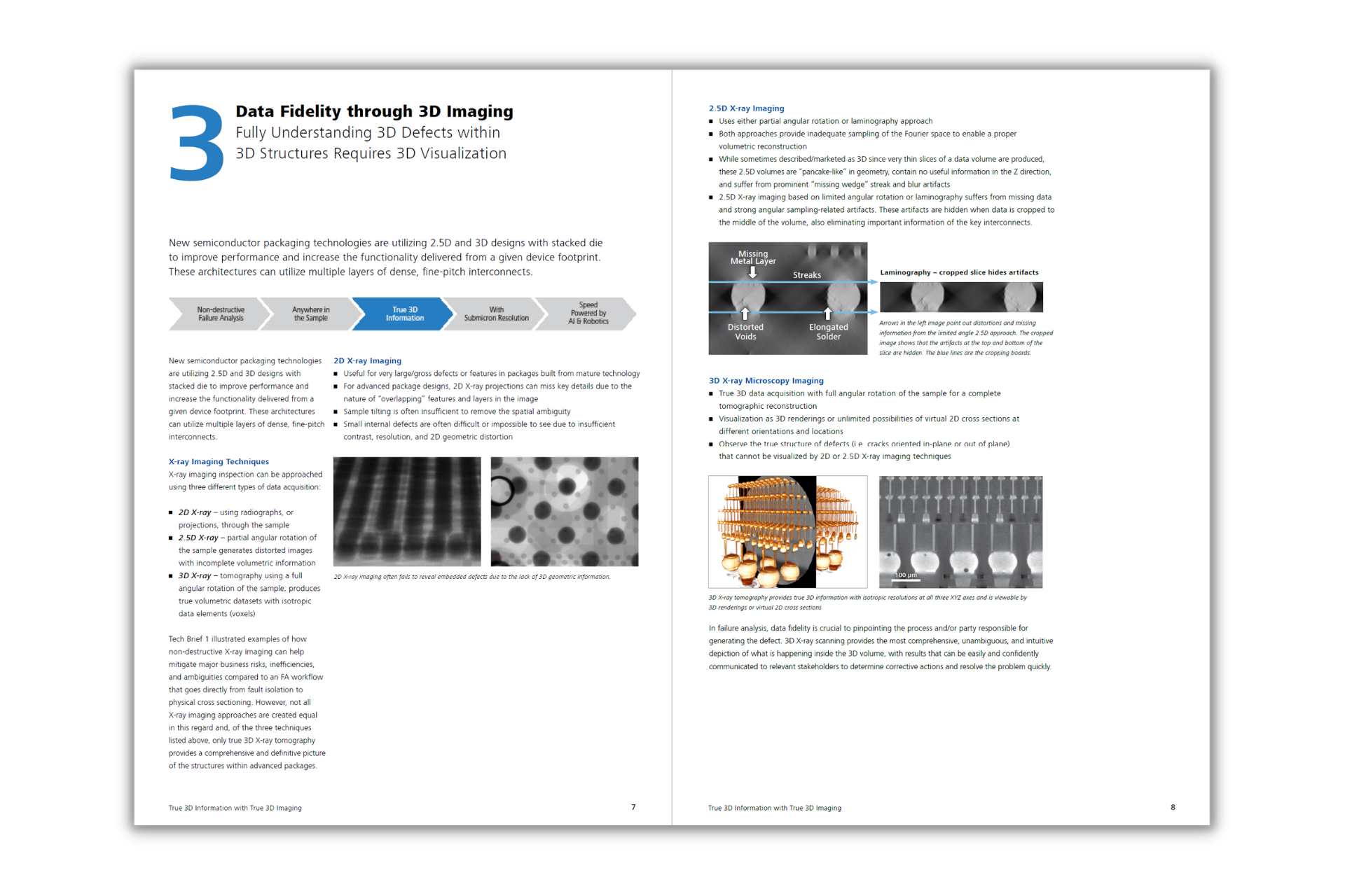
4. Learn how to apply 3D X-ray in failure analysis: The first document provides an in-depth look at the application of 3D X-ray in semiconductor package failure analysis. It outlines the advantages of 3D X-ray, such as non-destructive imaging and high resolution, as well as its limitations. Gaining a comprehensive understanding of 3D X-ray technology will help engineers make informed decisions when selecting the appropriate techniques for specific failure analysis tasks.
5. Learn how to utilize case studies and practical applications: Both documents provide several case studies and practical examples of failure analysis in semiconductor manufacturing. Engineers will learn about real-world applications of advanced techniques, such as XRM and DLHRR, and their effectiveness in various scenarios. Studying these case studies will help engineers better understand the practical implications and benefits of using these advanced techniques, which can assist them in applying these methods more effectively in their own work.