Semiconductor Failure Analysis
ZEISS Crossbeam Laser
FIB-SEM for high throughput sample preparation and nanoscale imagingParallel advances in FIB-SEM and ultra-fast lasers have radically changed sample preparation, characterization and failure analysis of semiconductor devices and packages.
Further enhance your productivity
With X-ray guided connected workflow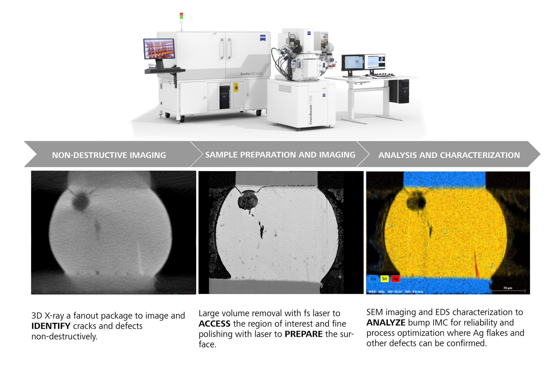


Download the correlative workflows for advanced packaging failure analysis
For efficient sample preparationAddition of a femtosecond laser to the ZEISS Crossbeam FIB-SEM improves the material removal rates up to 15 mio µm³ per second.
Sample preparation is efficient with minimal heat-affected zone due to the ultrashort pulse duration of the femtosecond laser.
This reduces sample preparation from hours or days to minutes without any artifacts. The laser preparation is suitable for several materials including silicon carbide and glass.