Clarity at Low Voltage Confidence at Every Layer
From passive voltage contrast to nanoprobing and defect localization, GeminiSEM 560 delivers high-resolution imaging on the most challenging semiconductor materials, without compromising surface integrity.


Clarity at Low Voltage
Confidence at Every LayerFrom passive voltage contrast to nanoprobing and defect localization, GeminiSEM 560 delivers high-resolution imaging on the most challenging semiconductor materials, without compromising surface integrity.


7 nm SRAM array imaged with Z and topographical contrast. Subtle failures require real surface sensitivity.
The Problem Isn’t Finding the Defect
It’s Seeing It ClearlyIn today’s semiconductor FA labs, surface sensitivity and material complexity are increasing faster than most imaging systems can handle.
Key challenges:
- Shrinking feature sizes across 3D architectures
- Beam-sensitive layers such as photoresists and low-k dielectrics
- ESD-related damage and delamination in stacked devices
- Need for non-destructive inspection at high contrast and low voltage
Every inaccurate scan increases turnaround time, jeopardizes yields, or leads to misdiagnosed failures.
Built to perform where other SEMs stall
especially at low voltage

Fine intermetallic layer detail imaged with GeminiSEM at low voltage. No sputter coating required.
Image Without Artifacts, Even at 70 V
GeminiSEM enables accurate topographic imaging and dimensional measurements without sputter coating, even on organic or beam-sensitive layers.
Use cases supported:
- High-resolution photoresist inspection between 70 and 800 V
- True surface characterization of uncoated samples
- Critical dimension (CD) inspection without deformation
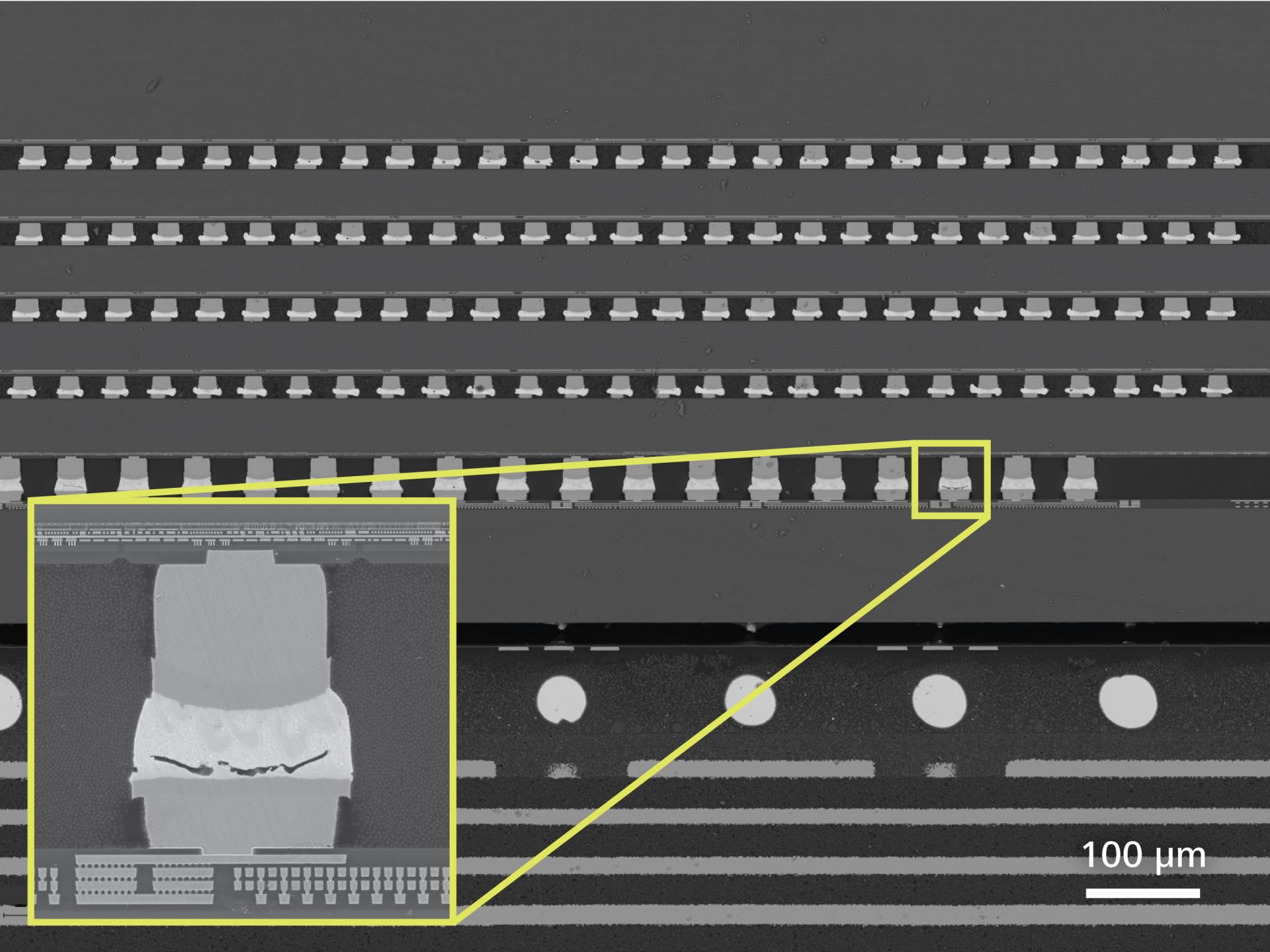

Extreme field of view imaging for 2.5D interconnect structures. Maintain resolution across the package.
Built for Semiconductor Workflows
GeminiSEM 560 supports high-resolution imaging across FA, device characterization, and electrical fault isolation.
- Supports nanoprobing and EBIC or EBAC
- Compatible with ZEISS FIB, TEM, XRM, and third-party tools
- Enables rapid scan-to-report with ZEN Connect
- Stable enough for 3 nm technology node and beyond
Ideal for:
- SiC and GaN power devices
- BEOL and FEOL structure validation
- WLCSP and 2.5D package inspection
- Electrical debug workflows with no imaging interference


Available with Local Support
GeminiSEM 560 is supported across Southeast Asia by experienced semiconductor specialists.
- Regional demo access
- Integration consulting
- Onsite and virtual training
- ZEISS service engineers familiar with power, RF, and automotive workflows
Get Sub-Nanometer Clarity. Without Compromise.
[Schedule a Demo]
[Get the Application Note PDF]
[Talk to a ZEISS Specialist]